


A stiffener is a rigid layer bonded to a flexible circuit to give local mechanical support. It exists because flex has one structural weakness: it cannot hold anything that needs to be pushed, pulled or inserted. A connector on unsupported flex peels off. A test pad on unsupported flex deforms under a probe. A component on unsupported flex cracks at the joint.
The decision is not whether to use a stiffener. It is where it goes, what it is made of, and how thick — and each of those has a failure mode if chosen carelessly.
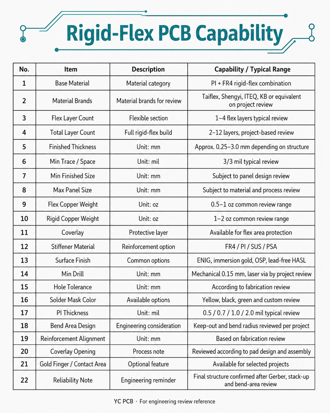
What Is the Purpose of a Stiffener?
Four functions, in order of frequency:
- Connector support — a ZIF, board-to-board or card-edge connector needs a rigid backing so insertion force does not delaminate the flex.
- Component mounting — SMT parts on flex need local rigidity, both for placement and for thermal cycling.
- Test pad support — probe pressure deforms unsupported flex, causing intermittent contact and pad damage.
- Assembly handling — a stiffened area gives the pick-and-place and fixture something to grip.
A stiffener is not a heat spreader (though aluminum can serve that role), and it is not a substitute for a proper rigid section in a rigid-flex design.
Material Options
Choose by function, not by habit
| Material | Thickness range | Stiffness | Best for | Watch out for |
|---|---|---|---|---|
| FR4 | 0.1–1.6 mm | Rigid, moderate CTE | General connector and component support; lowest cost | CTE mismatch with polyimide flex over wide temperature ranges |
| Polyimide (PI) | 0.05–0.5 mm | Semi-rigid, thin | Thin stacks, dynamic applications, close CTE match to flex | Less stiff; may not hold a heavy connector |
| Stainless steel | 0.1–0.3 mm | Very stiff, thin | Tight spaces needing high stiffness; shielding | Conductive — needs insulation; harder to process |
| Aluminum | 0.2–1.0 mm | Stiff, good thermal | Thermal spreading plus support; LED and power flex | Conductive; CTE mismatch; weight |
| Ceramic-filled FR4 | 0.2–1.0 mm | Very stiff, low CTE | High-reliability, thermal cycling | Cost and availability |
The selection usually follows one question: does the stiffener need to conduct heat or electricity? If no, FR4 is the cost-effective default. If the answer is thermal, aluminum. If the answer is "extreme stiffness in a thin stack", stainless steel with insulation.
Placement Rules
The boundary is the design decision
- Keep the stiffener edge at least one bend radius from the bend line. A rigid edge next to a flexible zone concentrates all strain at the boundary — the most common stiffener-related failure.
- Cover the connector footprint fully, plus a margin. A stiffener that ends mid-connector creates a hinge where the connector body meets the flex.
- Do not bridge two separate bend regions with one stiffener. You will create a rigid beam between two hinges and stress both.
- Account for adhesive flow. The bonding adhesive squeezes out during lamination, and the effective stiffener area is slightly larger than the drawn area.
- Consider both sides. Stiffeners on both sides move the neutral axis and change bending behaviour; on one side they create asymmetric stress.
- Leave a clear boundary in the drawing. The fabricator needs the stiffener area as a defined region with material and thickness, not as a note saying "reinforce here".
Connector Scenario Decision Table
| Scenario | Stiffener approach |
|---|---|
| ZIF connector, insertion force along the flex | FR4 or PI stiffener under the contact area, extending past the connector body |
| Board-to-board connector, repeated mating | Stiffener on the connector side, thickness matched to the mating height; consider both sides |
| Card-edge contact (gold fingers) | Stiffener behind the contacts, thickness set by the mating slot; hard gold on the contact side |
| SMT components near the connector | Extend the stiffener to cover both, or use two stiffeners with a defined gap |
| Test pads only | Thin PI stiffener is usually enough; FR4 if probe pressure is high |
| Dynamic bend near a connector | Stiffener must end at least a bend radius away; consider a longer flexible region instead |
| Thermal load (LED or power on flex) | Aluminum stiffener can double as a spreader, with insulation between |
What to Specify for a Quote
| Item | Detail |
|---|---|
| Stiffener material | FR4, PI, stainless steel, aluminum, or a specific grade |
| Thickness | Per stiffener, and the resulting total stack height |
| Area | A defined region on the drawing, with dimensions |
| Side | Top, bottom, or both |
| Adhesive type | If the application has temperature or outgassing constraints |
| Surface finish on the stiffener | If exposed (materials handling, marking) |
| Total thickness at the stiffener | Because it changes connector mating dimensions |
| Bend line locations | So the fabricator can check the clearance rule |
| Any electrical function | Grounding, shielding, thermal path |
| Panelisation impact | Stiffeners change panel stiffness and handling |
The most frequently missing item is total thickness at the stiffener. Connector mating dimensions depend on it, and a 0.2 mm error is a mechanical failure.
Where Stiffener Designs Fail
Edge at the bend. Already stated, and still the most common. It happens because the stiffener area is drawn from the connector outline rather than from the bend line.
Ignoring adhesive thickness. A 0.2 mm stiffener with 25 µm adhesive adds more than 0.2 mm to the stack. Multiply across a tolerance chain and the connector no longer mates.
Stainless steel without insulation. Stainless is conductive. If it sits over exposed traces or vias, you have a short waiting to happen.
Stiffener over a via. A via under a stiffener cannot be inspected or reworked, and the adhesive may not fill around it. Keep vias out of the stiffened area where possible.
Assuming stiffness equals flatness. A stiffener can lock in a warp if the lamination is not flat. For precision assemblies, ask about flatness after stiffening.
No finish specified on an exposed stiffener. An exposed FR4 stiffener with bare copper will oxidise; an exposed aluminum stiffener will scratch and corrode.
Design-to-Order Checklist
- Identify every location needing support: connectors, components, test pads, handling areas.
- Choose material by function — mechanical, thermal, or electrical.
- Set thickness from the mating dimension, not from what is in stock.
- Place every stiffener edge at least one bend radius from any bend line.
- Draw the stiffener area explicitly, with dimensions and side.
- State total stack thickness at the stiffener.
- Confirm adhesive type if temperature or outgassing matters.
- Keep vias and exposed traces out of stiffened regions, or insulate.
- Specify finish for any exposed stiffener surface.
- Confirm flatness requirement after stiffening for precision assemblies.
FAQ
What is a rigid-flex PCB?
A board built as one continuous stack-up with rigid sections (components, vias) and flexible sections (interconnect). In rigid-flex, the rigid sections are laminated structures, not bonded stiffeners — a distinction that matters for cost and reliability.
What does PCB stand for?
Printed Circuit Board. "Printed" refers to the additive/subtractive patterning of copper rather than drawn wiring.
Is a stiffener the same as a rigid section?
No. A stiffener is a separate piece bonded onto a finished flex; a rigid section is built into the stack-up during lamination. Stiffeners are cheaper and faster to change, rigid sections are more reliable and can carry vias. Choosing one when the design needs the other is a common and expensive mistake.
Can a stiffener be added after the flex is built?
Sometimes, for prototypes, but it is not a production approach. Adhesive bonding after the fact gives less control over flatness, adhesive thickness and registration, and the bond strength is lower than a laminated stiffener. Specify it on the drawing and let it be built in.
Why YC PCB
- 20+ years of PCB manufacturing including FPC and rigid-flex, with double-layer and 4-layer flex constructions
- Stiffener material, thickness and area confirmed at DFM review, with bend-line clearance checked
- Coverlay, stiffener and connector interface reviewed together, because they interact
- ENIG and hard gold finishes for contact areas
- AOI and electrical test on bare boards; X-Ray, ICT and FCT for assembly projects
- ISO 9001 and UL certification; NDA available for customer IP
Get a Quote — Send your Gerber, layer structure, stiffener material and thickness, connector specification and bend requirements. Our engineers reply with DFM notes, material options and pricing within one working day.


 English
 Japanese
 French
 German
 Spanish
 Italian
 Portuguese
 Russian
 Dutch
 Turkish
