

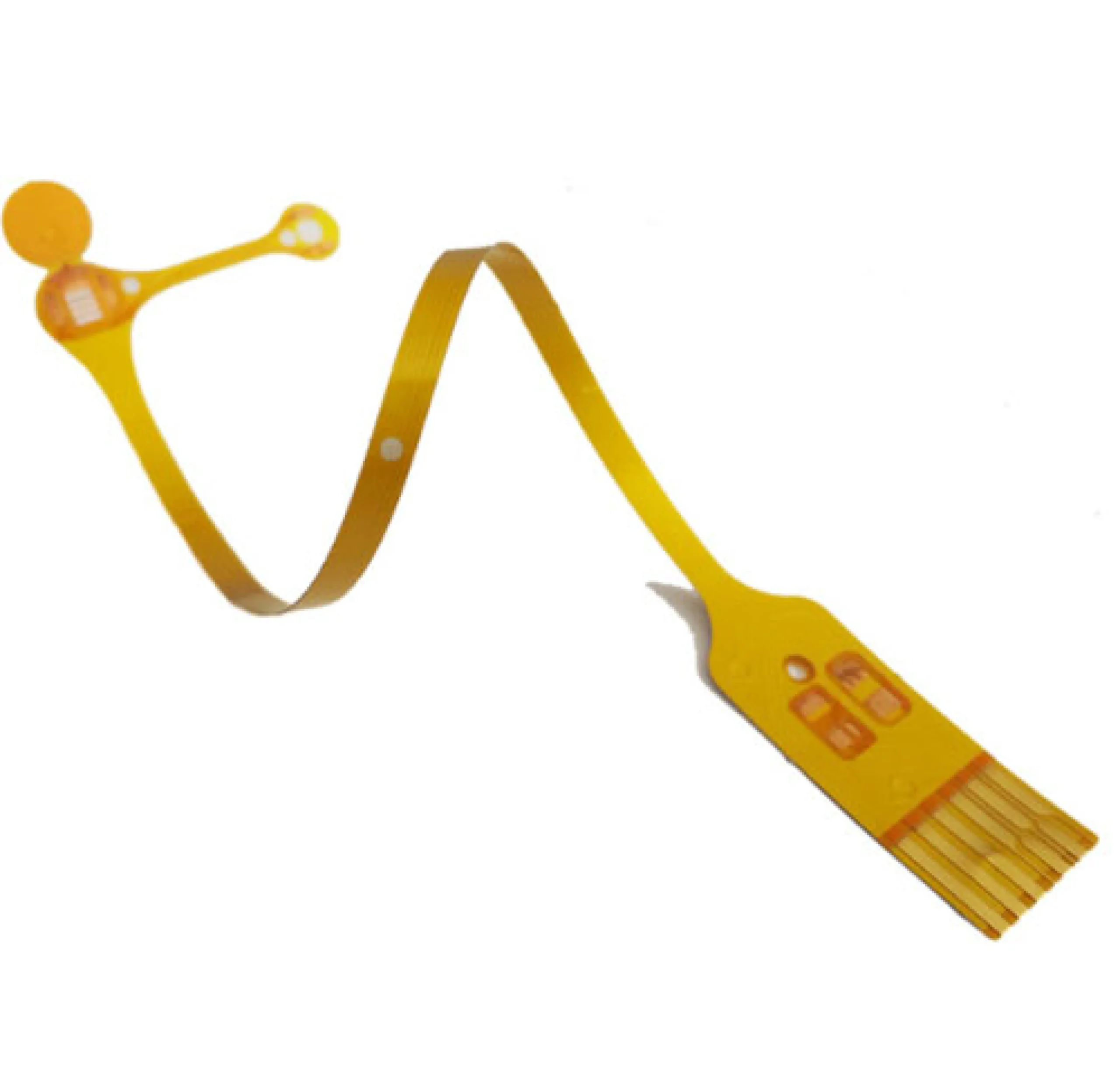
Flexible circuits fail in two places: the bend area, and the interface where the flex meets a connector or a rigid section. Not the circuit logic, not the layer count. Nearly every flex field failure traces back to a bend radius that was too tight, a copper trace running perpendicular to the bend, a coverlay opening that created a stress riser, or a stiffener that stopped exactly where the bending starts.
This guide covers flex design from the manufacturing side — the rules that decide whether the part can be built, assembled and cycled without cracking. YC PCB produces FPC and rigid-flex boards including double-layer and 4-layer flex constructions, and these are the review points that come up most often.

Static Bend vs Dynamic Bend: Decide This First
The one question that sets every other rule
Everything downstream depends on one question: will the flex bend once during assembly, or will it flex repeatedly in service?
| Static (install) bend | Dynamic (continuous) bend | |
|---|---|---|
| Bend cycles | One to a few, during assembly | Thousands to millions |
| Bend radius | Moderate; 1–2× material thickness is achievable in some builds | Much larger; typically 10× or more of the flex thickness |
| Copper type | Rolled annealed (RA) preferred, electrodeposited acceptable | Rolled annealed copper effectively required |
| Trace orientation | Perpendicular to bend is tolerable | Must run at an angle across the bend, never perpendicular |
| Coverlay | Standard | Thinner, more compliant, with careful opening design |
| Typical use | Camera modules, sensor connections, one-time fold assemblies | Print heads, hinge connections, moving arms, wearables |
A design that says "flexible PCB" without stating the bend type cannot be reviewed. This is the first question a fabricator will ask, and the answer changes the material, the copper and the cost.
Bend Radius and Cycle Life: The Numbers to Design To
Bend radius is usually written as a multiple of the total flex thickness, not as a millimetre figure, because the same radius is benign on a thin single-sided flex and severe on a 4-layer build. The bands below are the industry rules of thumb used in flex design review; treat them as a starting point to confirm against your actual build, not as a guarantee.
| Bending regime | Radius to flex thickness | Copper | Expected life |
|---|---|---|---|
| Single fold during assembly, no service flexing | ~1× or slightly more | ED acceptable | One cycle, no fatigue requirement |
| Flex-to-install, occasional service movement | ~5–10× | RA preferred | Tens to low hundreds of cycles |
| Continuous dynamic flexing | ~10× or greater; more for multilayer | RA required | Thousands to millions, depending on strain |
| Multilayer dynamic (3+ conductor layers) | Substantially larger than single-layer guidance | RA required, balanced construction | Falls faster than layer count rises |
What actually governs cycle life
Four variables decide whether a dynamic bend survives a million cycles or ten thousand:
- Strain in the copper. Roughly, the outer copper sees strain proportional to its distance from the neutral axis divided by the bend radius. Halving the radius doubles the strain — which is why radius is the dominant lever, not copper thickness.
- Copper type. Rolled annealed copper has grain structure aligned with the rolling direction and tolerates repeated bending far better than electrodeposited copper, which is brittle at the grain boundaries.
- Position in the stack. Copper furthest from the neutral axis sees the highest strain. In a symmetric 2-layer flex, both outer layers are equally exposed; in an asymmetric build, one side fails first.
- Bend line quality. A coverlay opening, a stiffener edge or a via near the bend line raises local strain sharply and shortens life by an order of magnitude, regardless of radius.
If you cannot reach the radius
When mechanics force a tighter bend than the guidance allows, the practical options are to reduce flex thickness (fewer copper layers, thinner coverlay), switch to RA copper, move the bend line away from every stiffener and opening, or add a formed bend with a permanent set rather than a free bend. What does not work is keeping the design and asking for a longer-life build — life is set by strain, and strain is set by geometry.
Bend Area Design Rules
- Never run a trace perpendicular across a bend. Route at 45° or parallel to the bend line, distributing strain along the trace rather than concentrating it at one point.
- Widen the trace in the bend, do not narrow it. A wider trace distributes strain; a necked-down trace becomes the failure point.
- Avoid plated through-holes in or near the bend. A PTH is a rigid inclusion in a flexible region and will crack. Move vias out of the bend area, or use a rigid-flex design with a rigid section for the vias.
- Round all internal corners in the bend region. A sharp inside corner is a stress riser; a generous radius spreads the load.
- Keep the bend region free of copper pour. Solid copper in a bend stiffens locally and forces the strain into adjacent areas.
- Define the bend line on the drawing. A mechanical drawing with the bend location, radius and direction is part of the design data, not an optional extra.
Coverlay vs Solder Mask
Why the choice is mechanical, not cosmetic
Flex circuits usually use coverlay (a laminated polyimide film with adhesive) rather than solder mask. The difference is mechanical, not cosmetic:
| Property | Coverlay | Solder mask on flex |
|---|---|---|
| Flexibility | High; moves with the circuit | Limited; cracks under repeated bending |
| Thickness | 25–50 µm film plus adhesive | Thin, but brittle |
| Opening definition | Mechanical or laser cut; larger clearance needed | Photolithographic, tighter |
| Cost | Higher, more process steps | Lower |
| Best use | Any flexing area, dynamic bends | Static, low-bend, cost-sensitive designs |
Coverlay openings need more clearance than solder mask openings because the adhesive flows during lamination. Design pad openings accordingly, and never place a coverlay opening edge across a bend.
Stiffeners: Where They Help and Where They Hurt
The boundary is the risk, not the stiffener
A stiffener is a rigid layer bonded to a flex to support connectors, component areas or test pads. It solves a real problem — unsupported connectors peel off flex — and creates a new one if placed carelessly.
Rules:
- Stiffener edges must not sit at the bend line. A rigid edge adjacent to a flexible zone concentrates all strain at the boundary. Keep the stiffener edge at least a bend radius away.
- Stiffener material matters. FR4, polyimide and stainless steel are common; each has a different CTE and stiffness. Match it to the assembly process.
- Thickness affects connector height. A stiffener changes the stack height at the connector, which changes the mating dimension.
- Stiffener on both sides versus one side changes the neutral axis and therefore the bend behaviour.
- Adhesive flow can create a fillet that affects flatness. Specify the stiffener area and thickness on the drawing.
Component and Pad Rules
- Keep components off the bend area entirely. Even a small chip component creates a rigid island.
- Anchor pads with teardrops where the trace enters a pad, to reduce stress concentration.
- Use rounded pads rather than sharp rectangles on flex when the process allows.
- Consider polyimide-based stiffeners or local bonding for components near bend transitions.
- Design test pads with adequate support, or they will deform under probe pressure.
What the Fabricator Needs to Quote a Flex
| Input | Detail required |
|---|---|
| Gerber and drill | Single revision, all layers including coverlay openings |
| Board outline | Including the bend region and any cut-outs |
| Layer structure | Number of conductive layers, coverlay on which sides, stiffener locations |
| Bend requirement | Static or dynamic, bend line location, radius, direction, cycle count if dynamic |
| Coverlay spec | Material, thickness, opening definition |
| Stiffener spec | Material, thickness, area, adhesive type |
| Surface finish | ENIG is common on flex; specify if hard gold is needed for contacts |
| Connector interface | Type, position, insertion direction, any reinforcement requirement |
| Assembly boundary | Where the part is gripped or supported during assembly |
| Panelisation | Array format and any handling constraints |
A flex RFQ without bend information is a fabrication quote, not a product quote. The two are not the same number.
Where Flex Designs Fail in Production
Bend radius defined by mechanics after the flex is designed. The flex should be designed to the radius, not adapted to it. Reducing radius after layout means re-routing the bend area.
Coverlay opening across a bend. This is the single most common cause of flex cracking. The opening creates an exposed, unreinforced strip exactly where strain is highest.
Stiffener edge at the bend. Same mechanism, different component. Both are drawing errors, both are cheap to fix before tooling.
Adhesive squeeze-out ignored. Coverlay adhesive flows during lamination and can reduce the effective opening. Opening dimensions must account for it.
Panel handling assumed. Thin flex panels distort during processing. Panelisation and carrier design affect yield more than on rigid boards.
Impedance assumed to be free. Controlled impedance on flex is achievable but the dielectric is thin and Dk differs from FR4. It needs its own stack-up and coupon.
Design-to-Order Checklist
- State static or dynamic bending, with radius, direction and cycle count.
- Route bend-area traces at an angle, widened, never perpendicular.
- Remove PTHs, pours and components from the bend region.
- Choose coverlay for any flexing area; reserve solder mask for static, low-bend designs.
- Place stiffeners away from the bend line by at least a bend radius.
- Round internal corners and add teardrops at pad entries.
- Provide a mechanical drawing showing bend line, stiffener area and connector interface.
- Specify coverlay material and thickness, and account for adhesive flow.
- State the assembly boundary so the fabricator knows where the part is supported.
- Confirm panelisation and handling with the fabricator before tooling.
FAQ
What bend radius should I specify for a dynamic flex?
Start from the multiple of total flex thickness, not from a millimetre figure: roughly 10× or more for continuous flexing, with more margin for multilayer builds. Then check the four variables that actually govern life — copper type, copper position in the stack, bend line clearance and strain. Confirm the final value with the fabricator against the real stack-up.
Why does rolled annealed copper matter so much on flex?
Because grain structure controls fatigue. Rolled annealed copper has grains elongated along the rolling direction, so repeated bending distributes strain instead of concentrating it at grain boundaries. Electrodeposited copper is columnar and brittle in that direction, which is why it is acceptable for a single fold and unsuitable for continuous flexing.
Can I use solder mask instead of coverlay to save cost?
Only on static, low-bend designs. Solder mask is thin and brittle, and cracks under repeated bending, exposing copper exactly where strain is highest. For anything that flexes in service, coverlay is not a premium option — it is the functional requirement.
How far should a stiffener be from the bend line?
At least one bend radius, and preferably more. The stiffener edge is where flexibility stops, so it is where strain concentrates. A rigid edge sitting at the bend line is one of the two most common causes of flex cracking, together with a coverlay opening across the bend.
Why YC PCB
- 20+ years of PCB manufacturing including FPC and rigid-flex, with double-layer and 4-layer flex constructions
- Coverlay, stiffener and bend-area requirements reviewed at DFM stage, before tooling
- Rigid-flex builds that place vias and components in rigid sections while keeping interconnects flexible
- ENIG and hard gold finishes suitable for flex contacts
- Impedance control available on multilayer flex with a dedicated stack-up
- AOI and electrical test on bare boards; X-Ray, ICT and FCT for assembly projects
- ISO 9001 and UL certification; NDA available for customer IP
Get a Quote — Send your Gerber, layer structure, bend requirement and stiffener specification with quantity and target date. Our engineers reply with DFM notes, material options and pricing within one working day.


 English
 Japanese
 French
 German
 Spanish
 Italian
 Portuguese
 Russian
 Dutch
 Turkish
