

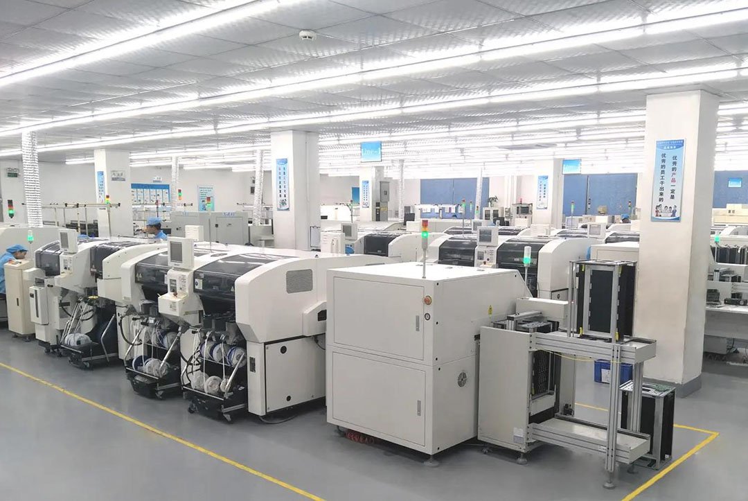
Most PCB assembly process articles describe the machine sequence: print paste, place parts, reflow, inspect. Accurate, and not the part that decides whether your order goes smoothly. What decides that is the input set you provide and the inspection points you agree to — because every assembly defect that reaches you was either caused by an input error or passed through an inspection that was not specified.
This article maps the assembly process as a buyer experiences it: files in, process stages, inspection gates, deliverables out. YC PCB runs turnkey assembly with SMT, THT and mixed technology, including BGA, QFN and Micro-BGA packages with X-Ray inspection.
What Files Does PCB Assembly Require?
| File | Purpose | Common mistake |
|---|---|---|
| Gerber (RS-274X) | Fabrication of the bare board | Outdated revision mixed with the current one |
| Excellon drill | Hole sizes and positions | Missing or mismatched with pad sizes |
| BOM | Components: reference, value, package, quantity, MPN | Missing MPN, or a value-only BOM that forces substitution |
| Centroid / CPL / pick-and-place | X-Y coordinates and rotation per reference | Rotation convention mismatch (0° reference differs between CAD tools) |
| Assembly drawing | Polarity, orientation, special instructions | Absent, so polarised parts are placed on assumption |
| Test specification | What "pass" means | Absent, so "inspection" defaults to visual only |
| Panelisation / array drawing | How boards sit in the frame | Missing, so fiducials and break-away are improvised |
The centroid rotation convention is the single most common cause of a first-article failure. Different CAD tools export rotation with a different zero reference, and a part rotated 90° looks correct in the file and wrong on the board.
The Assembly Process, Stage by Stage
The machine sequence, and where it is inspected
| Stage | What happens | Inspection gate |
|---|---|---|
| File and DFM review | Gerber, BOM, CPL and drawing checked for consistency | Engineering sign-off before material is ordered |
| Component sourcing | Parts purchased or kitted; alternates confirmed | BOM match report, lifecycle check |
| Bare board fabrication | The PCB is built to the fabrication drawing | Electrical test, AOI |
| Solder paste printing | Paste deposited through a stencil | SPI (solder paste inspection): volume, height, alignment |
| SMT placement | Components placed by pick-and-place | Pre-reflow visual or inline inspection |
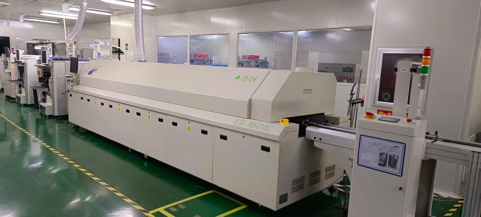
| Reflow | Paste melts and forms joints | Post-reflow AOI |
| THT / DIP assembly | Through-hole parts inserted and wave or selective soldered | Visual and, where required, X-Ray |
| Cleaning | Flux residue removed where the process requires it | Cleanliness check for conformal-coated or high-impedance boards |
| X-Ray inspection | Hidden joints: BGA, QFN, Micro-BGA | Void percentage, bridging, alignment |
| Electrical test | ICT or flying probe on assembled boards | Pass/fail per net |
| Functional test (FCT) | Board powered and exercised | Per test specification |
| Programming and final assembly | IC programming, conformal coating, box build as scoped | Per scope |
| Packing and shipping | ESD-safe packaging, moisture barrier where required | Shipping inspection |
What Is SPI and Why Does It Come First?
Solder paste inspection measures the paste deposit — volume, height, area and alignment — immediately after printing and before placement.
It matters because most solder defects originate at the printing step, not the placement step. Insufficient paste causes opens; excess causes bridging; misalignment causes tombstoning and skew. Catching these before reflow means the board can be cleaned and reprinted rather than scrapped.
A supplier who prints without SPI is relying on AOI after reflow, which only detects the consequence, not the cause. For fine-pitch and BGA work, SPI is not optional.
Input, Output and Pass Criteria for Each Stage
This is the table most process articles never publish. For each stage it states what goes in, what comes out, and what "pass" actually means — which is the only way to tell whether an inspection is real or nominal.
| Stage | Input | Output | Pass criteria |
|---|---|---|---|
| File and DFM review | Gerber, drill, BOM, CPL, drawing | DFM report, resolved questions, approved file set | No open question at release; revision locked |
| Component sourcing | Approved BOM with MPNs | Kitted or purchased parts, alternates list | Every line matched or an approved alternate recorded |
| Paste printing | Stencil, paste, panel | Deposited paste per pad | Volume, height and offset within agreed limits on all critical pads |
| SMT placement | Programmed machine, feeders | Placed components before reflow | No missing, offset or rotated part outside tolerance |
| Reflow | Profiled oven | Formed solder joints | Profile within the window on the real board; no bridging, tombstoning or cold joint |
| THT and selective solder | Inserted parts, solder | Filled barrels, fillets | Fillets on both sides where required; no voids or flags |
| X-Ray | Assembled board | Images of hidden joints | Void percentage and alignment within the agreed limit; no bridging under BGA |
| Electrical test | Netlist, fixture or probe program | Pass/fail per board | 100% of nets tested; failures segregated, not reworked silently |
| Functional test | Test spec, power, loads | Verified behaviour | Meets the written spec, including any programmed firmware version |
Two rows deserve emphasis. Electrical test on bare boards is not the same as test on assemblies — a bare board test proves copper continuity, while assembly test proves the joints. And "no bridging" is not a pass criterion for a BGA unless someone stated a void percentage, because bridging under a package is invisible to both AOI and the operator.
How Long Does PCB Assembly Take?
Any specific number given before the files are reviewed is a placeholder. Real lead time depends on:
- Component availability — this dominates. A single long-lead part can set the entire schedule, and lifecycle or allocation issues can add weeks.
- Bare board lead time — which depends on layer count, material and finish.
- Placement count and mix — a dense single-sided SMT board and a mixed SMT/THT board with connectors are different programmes.
- Stencil and fixture fabrication — one-time items with their own lead time.
- Test scope — ICT fixtures take longer to build than functional test cables.
- First-article approval — if the first article needs your sign-off, the loop adds calendar time.
- Programming and coating — each added scope adds a step and a queue.
The practical sequence: send the full package, get a BOM availability check and a schedule tied to specific conditions, then re-confirm after components are booked.
How Much Does PCB Assembly Cost?
Eight cost drivers, in order of impact
Assembly cost is not area-based like bare PCB. It is driven by:
- Components — often the largest line item, and the most volatile
- Placement count — cost scales with the number of placements, not board size
- Package difficulty — fine-pitch BGA, QFN and 01005 parts cost more per placement than 0805 passives
- SMT / THT mix — through-hole and mixed technology add hand or selective soldering steps
- Stencil and fixtures — one-time, amortised over the order
- Test scope — SPI, AOI, X-Ray, ICT, FCT each add cost and time
- Quantity — setup cost per order is fixed, so small runs carry a high per-unit share
- Double-sided assembly — two passes, two reflows, roughly double the process time
The cheapest quote is usually the one with the narrowest scope. Compare quotes by scope, not by total.
What Is the 3W Rule in PCB?
A design rule, not an assembly rule: keep centre-to-centre spacing between adjacent traces at three times the trace width to reduce crosstalk. It belongs to layout, but it interacts with assembly — tight spacing constrains stencil aperture design and increases bridging risk at fine pitch.
If a design uses spacing well below 3W in dense areas, mention it at quotation so stencil and process can be adjusted.
Where Assembly Programmes Go Wrong
BOM and CPL do not match. A reference designator in the BOM that does not exist in the CPL, or a package mismatch between the two, stops the programme at file review.
Value-only BOMs. Without an MPN, the supplier chooses the part. That is a specification decision you have delegated without knowing it.
No assembly drawing for polarised parts. Diodes, electrolytics, connectors and LEDs all have orientation. Without a drawing, orientation is an assumption.
Test spec left to the supplier. "Tested" can mean visual inspection. If you need ICT or FCT, say so, and define the pass criteria.
Alternates approved verbally. A verbal "any equivalent is fine" becomes a sourcing decision with no record. Use a written alternate list.
Conformal coating scoped late. Coating changes handling, masking, inspection and rework. Scoping it after the first build usually means rebuilding.
First article not required. For a new design, a first-article inspection with a photo report is the cheapest insurance in the programme.
Buyer Checklist for an Assembly Order
- Confirm the file set: Gerber, drill, BOM with MPNs, centroid/CPL, assembly drawing, test spec.
- Ask for a BOM availability and lifecycle check before the quote is finalised.
- Agree the alternate-part rule in writing.
- Confirm the inspection gates: SPI, AOI, X-Ray, ICT, FCT — and who pays for each.
- Confirm whether a first article with photo report is included.
- Scope everything outside standard assembly: programming, coating, box build, labelling, packaging.
- Confirm the schedule drivers and re-confirm after components are booked.
- Agree the acceptance criteria and the rework policy before the build starts.
FAQ
What does turnkey PCB assembly include?
Everything from bare board to tested assembly: board fabrication, component sourcing, stencil, SMT and THT assembly, reflow, inspection and the agreed test scope. Partial turnkey means you supply some of it — usually the components — and consignment means you supply all material. The scope boundary decides who carries component risk.
What is the difference between ICT and FCT?
ICT checks the physical assembly against the netlist — opens, shorts, wrong or missing values, using a bed-of-nails fixture. FCT powers the board and exercises it functionally, checking behaviour rather than continuity. ICT costs more to set up because of the fixture; FCT needs a written test spec. They find different defects and are not substitutes.
Can you assemble boards with components I supply?
Yes, and the practical consequence is that component risk stays with you. Missing, damaged or counterfeit parts found at assembly become a schedule problem rather than a supplier problem. If you consign, send a counted kit with margin, and agree in writing who absorbs attrition and who verifies authenticity.
What is the most common assembly defect?
Insufficient or misaligned solder paste, followed by component rotation from a CPL convention mismatch. Both are caught before reflow if SPI and a first-article check are in scope. Both become scrap or rework if the only inspection is visual after reflow.
Why YC PCB
- 20+ years of PCB and PCBA manufacturing, exporting to 20+ countries
- Turnkey assembly: SMT, THT/DIP, mixed technology, and BGA/QFN/Micro-BGA support
- BOM management and component sourcing, with alternates confirmed before build
- Inspection chain includes AOI, electrical test, X-Ray, ICT and FCT per project scope
- IC programming and box build available as defined scope extensions
- DFM/DFA review before production; NDA available for customer IP
- ISO 9001 and UL certification; RoHS compliance documentation on request
Get a Quote — Send your Gerber, BOM, centroid file, assembly drawing and test requirement with quantity and target date. Our engineers reply with a BOM check, DFM notes and pricing within one working day.


 English
 Japanese
 French
 German
 Spanish
 Italian
 Portuguese
 Russian
 Dutch
 Turkish
