
はじめに:
Printed Circuit Board (PCB) assembly is a critical process in the manufacturing of electronic devices, enabling the interconnection of various electronic components to create functional and reliable devices. Whether it's a smartphone, a computer, or an advanced industrial machine, PCB assembly plays a vital role in bringing these devices to life. This article provides a comprehensive guide to PCB assembly, covering the key stages involved in transforming a design into a fully functional PCB assembly.
設計段階:
PCB組立の旅は設計段階から始まります。この段階では、電気技師や設計者が専門的なソフトウェアツールを使用して、回路図とPCBのレイアウトを作成します。彼らは、適切な機能性と信号の整合性を確保するために、部品の配置、配線経路、信号トレースを定義します。.
部品選定と調達:
設計が確定したら、次のステップはPCBに搭載される電子部品の選定です。部品選定には、機能性、信頼性、入手性、コストなどの要素を考慮します。部品が選ばれたら、信頼できる供給業者や販売代理店から調達する必要があります。.
PCB製造:
With the components in hand, the PCB fabrication process begins. This involves producing the actual circuit board based on the design specifications. The fabrication process typically includes steps such as substrate material selection, layer stacking, etching, drilling, plating, and soldermask application. Advanced fabrication techniques, such as multilayer PCBs and surface-mount technology (SMT), are commonly used to accommodate complex designs and miniaturized components.
部品配置:
PCBが製造されたら、次の段階は部品の配置です。このステップでは、自動化された装置や手作業を使用して、電子部品を正確にPCBに配置します。表面実装技術(SMT)は、その高効率、正確さ、および小型化された部品の取り扱い能力から広く使用されています。スルーホール技術(THT)は、大型部品や特定の用途に使用される代替方法です。.
はんだ付けとリフロー:
部品配置の後、はんだ付けが行われ、部品とPCBの間に電気的および機械的な接続を確立します。はんだペーストは、はんだ合金粒子とフラックスの混合物であり、はんだパッドに塗布されます。その後、PCBはリフロー工程にかけられ、加熱してはんだペーストを溶かし、強固で信頼性の高いはんだ接合を作ります。赤外線加熱、蒸気相、対流リフローなど、さまざまな方法が製造要件に応じて使用されます。.
検査とテスト:
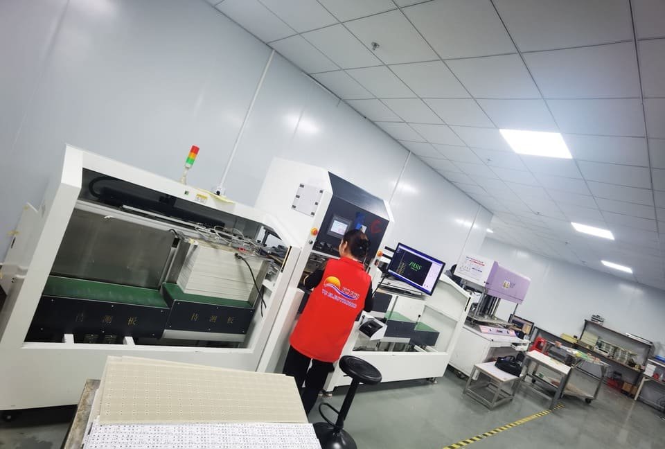
Quality control is a crucial aspect of PCB assembly. Once the soldering process is complete, the assembled PCBs undergo thorough inspection and testing. Automated optical inspection (AOI) systems are commonly used to detect defects such as misalignment, missing components, solder bridges, or open circuits. Functional testing is also conducted to ensure that the PCB operates as intended, verifying the electrical connections, signal integrity, and overall performance.
梱包と出荷:
検査とテストの後、PCB組立品は梱包と出荷の準備をします。これには、PCBの洗浄、フラックス残留物の除去、耐久性と信頼性を高めるためのコンフォーマルコーティングや保護フィルムの塗布が含まれます。完成したPCB組立品は丁寧に梱包され、最終的な電子機器に組み込むか、顧客に出荷される準備が整います。.
結論:
PCB組立は、電子機器に命を吹き込む複雑で重要なプロセスです。最初の設計段階から最終的な梱包と出荷まで、各段階には正確さ、細部への注意、品質基準の遵守が求められます。この記事で示された包括的なガイドに従うことで、メーカーはPCBの成功裏の組立を確実にし、機能的で信頼性の高い高品質な電子機器を作り出し、現代の世界を支えています。.
 Japanese
  English
  French
  German
  Spanish
  Italian
  Portuguese
  Russian
  Dutch
Dutch  Turkish