

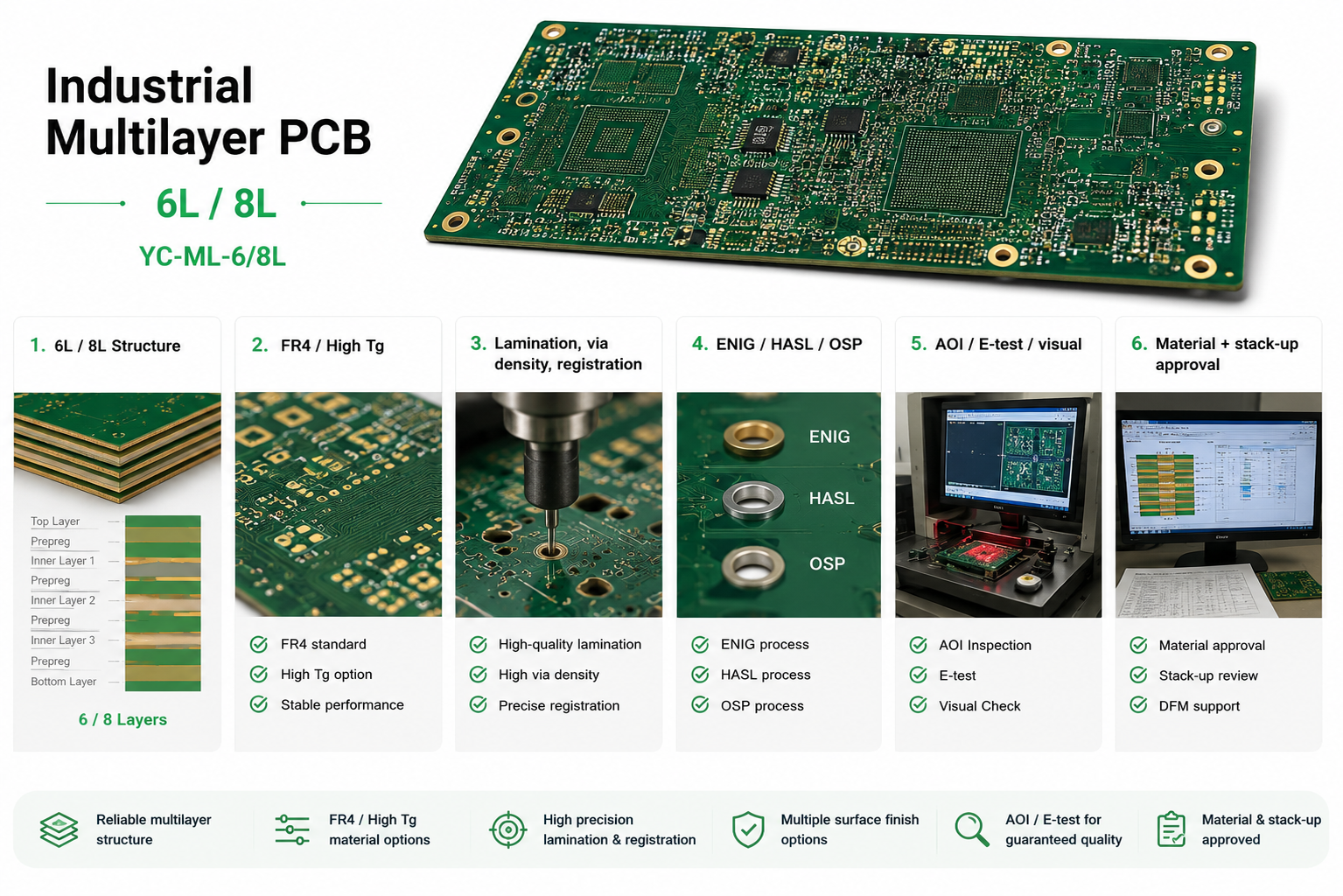
Multilayer design guides usually explain what a reference plane is and why you should not split a ground plane. Useful, but by the time a design reaches the fabricator, those decisions are already made. What determines whether the board can be built reliably — and at what yield — is a much narrower set of choices: layer count and sequence, stack-up symmetry, via structure, copper balance, and the data you supply.
This guide covers multilayer PCB design from the manufacturing side. YC PCB builds 6- to 32-layer rigid boards and HDI, and the questions below are the ones that come back from our engineering review most often.
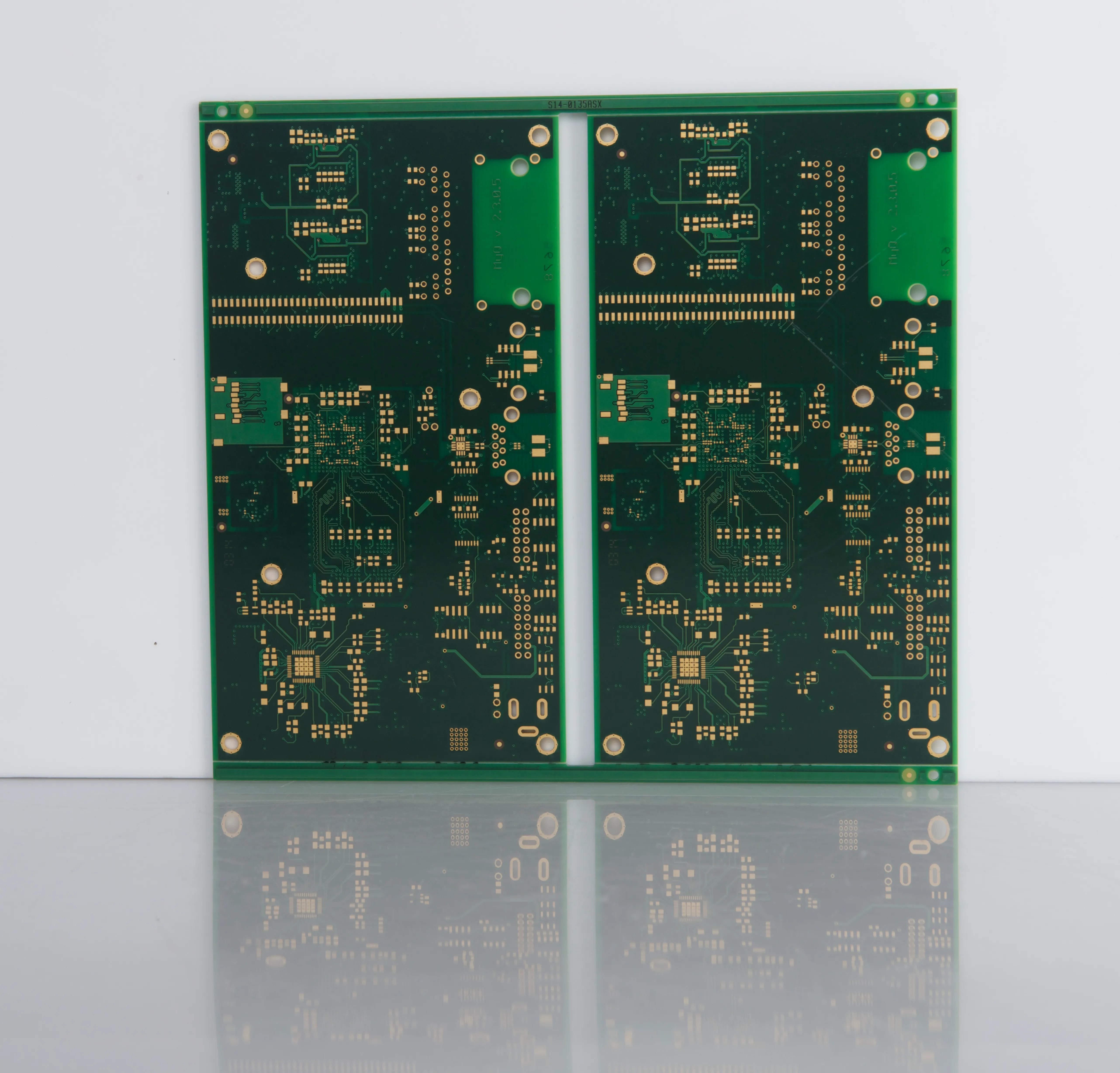
How Many Layers Does Your Design Actually Need?
The four pressures that drive layer count
Layer count is not a status symbol. It is the outcome of four pressures:
- Routing density — how many traces must cross a given area
- Reference planes — high-speed signals need a continuous return path adjacent to them
- Power distribution — separate power planes reduce impedance and decoupling complexity
- Pin count and package pitch — fine-pitch BGA fan-out consumes layers fast
A common and expensive mistake is to add layers to solve a density problem that is actually a placement problem. If components are clustered so that a large net must cross the entire board, two more layers will not fix it — moving the connector will.
The practical sequence: place and route on the minimum stack-up, count the layers you actually needed, then add one spare pair if the product will be revised. Designing at exactly the limit leaves nothing for ECOs.
What each additional pair of layers buys you
Adding layers is not linear. Each pair does a specific job, and the cost of the next pair jumps when the fabrication route changes.
| Layer count | What it typically buys | Main engineering gate | Cost / schedule behaviour |
|---|---|---|---|
| 2 | Routing only, no planes | Etch resolution on 1 oz | Baseline; single lamination, no bonding step |
| 4 | Two routing + power/ground plane | Plane integrity, via aspect ratio | Modest step up; still one lamination cycle |
| 6 | Two routing pairs + planes, better shielding | Symmetry control, registration | Standard industrial stack-up; small step from 4 |
| 8–10 | Fine-pitch fan-out, multiple planes | Drill aspect ratio, impedance tolerance | Each pair adds material and lamination time |
| 12–16 | Dense BGA escape, multiple impedance classes | Layer registration, thickness control | Cost rises faster than layer count suggests |
| 18–24 | Very dense or high-layer-count industrial designs | cURL Too many subrequests by single Worker invocation. To configure this limit, refer to https://developers.cloudflare.com/workers/wrangler/configuration/#limits | cURL Too many subrequests by single Worker invocation. To configure this limit, refer to https://developers.cloudflare.com/workers/wrangler/configuration/#limits |
| 26–32 | cURL Too many subrequests by single Worker invocation. To configure this limit, refer to https://developers.cloudflare.com/workers/wrangler/configuration/#limits | cURL Too many subrequests by single Worker invocation. To configure this limit, refer to https://developers.cloudflare.com/workers/wrangler/configuration/#limits | cURL Too many subrequests by single Worker invocation. To configure this limit, refer to https://developers.cloudflare.com/workers/wrangler/configuration/#limits |
Two things drive the step changes. First, lamination cycles — everything up to a single press is one class of work, and beyond that you are stacking process risk. Second, registration capability — as layer count rises, every layer must align to the same datum, and the fabricator's registration tolerance becomes the limiting number for annular ring.
Stack-Up Symmetry: The Cheapest Reliability Decision
What symmetry actually means
A multilayer stack-up should be symmetric about the centre in both copper distribution and dielectric thickness. Asymmetric stack-ups warp during lamination and again during reflow.
| Stack-up pattern | Behaviour | Practical note |
|---|---|---|
| Symmetric copper, symmetric dielectric | Low warp, predictable | The default for anything 6 layers and above |
| Symmetric dielectric, asymmetric copper | Warp risk after reflow | Common when one plane is a solid pour and the other is routed |
| Asymmetric dielectric | High warp, thickness drift | Avoid unless mechanics force it |
| Balanced with thieving | Controlled | Copper balancing adds design time and saves yield |
Warpage limits are usually quoted as a percentage of diagonal length, and assembly equipment is less forgiving than the fabrication standard. If the board will go through a printer with tight edge support, ask for the warp figure, not just compliance.
How warp is measured, and why your figure differs
Warp and twist are measured on a flat plate after the board has been thermally stressed, then expressed as a percentage of the diagonal. That definition matters twice. It is measured after stress, so a board that is flat on delivery can still fail at reflow. And because it is a proportion of the diagonal, a long narrow board and a square board carry different absolute allowances at the same percentage. If your fixture clamps only two edges, the number that matters is the bow across the unsupported span, not the whole panel.
When you cannot be symmetric
Mechanics, connectors or a single large heatsink pad sometimes force an imbalance. The options, in order of preference:
- Rebalance with copper thieving on the sparse side — cheap, done at design time, no process penalty.
- Rebalance with dielectric — thicken the thin side slightly so Z-axis expansion is symmetric even if copper is not.
- Accept the imbalance and declare it before tooling — the fabricator can adjust press parameters for a known condition.
- Accept the warp and design the fixture around it — legitimate for small boards, expensive for large ones.
What does not work is shipping an asymmetric design and asking the fabricator to "make it flat". Warp is a property of the build-up, not a defect the router can remove.
cURL Too many subrequests by single Worker invocation. To configure this limit, refer to https://developers.cloudflare.com/workers/wrangler/configuration/#limits
cURL Too many subrequests by single Worker invocation. To configure this limit, refer to https://developers.cloudflare.com/workers/wrangler/configuration/#limits
cURL Too many subrequests by single Worker invocation. To configure this limit, refer to https://developers.cloudflare.com/workers/wrangler/configuration/#limits
- cURL Too many subrequests by single Worker invocation. To configure this limit, refer to https://developers.cloudflare.com/workers/wrangler/configuration/#limits cURL Too many subrequests by single Worker invocation. To configure this limit, refer to https://developers.cloudflare.com/workers/wrangler/configuration/#limits.
- Blind and buried vias cURL Too many subrequests by single Worker invocation. To configure this limit, refer to https://developers.cloudflare.com/workers/wrangler/configuration/#limits.
- cURL Too many subrequests by single Worker invocation. To configure this limit, refer to https://developers.cloudflare.com/workers/wrangler/configuration/#limits cURL Too many subrequests by single Worker invocation. To configure this limit, refer to https://developers.cloudflare.com/workers/wrangler/configuration/#limits.
cURL Too many subrequests by single Worker invocation. To configure this limit, refer to https://developers.cloudflare.com/workers/wrangler/configuration/#limits.
Copper Weight and Balance
How trace/space quietly shrinks
Copper weight affects three things beyond current capacity: etch resolution, lamination pressure, and thermal mass during assembly.
- Minimum trace/space shrinks as copper thickens. A fabricator holding 4/4 mil at 1 oz may only hold 6/6 mil at 2 oz. Confirm this per order.
- Large copper pours change the thermal profile. A board with heavy ground pour on one side and sparse routing on the other behaves differently in reflow.
- Thieving and balancing are not cosmetic. They equalise plating current density and reduce warp.
If your design has a deliberate copper imbalance — a big thermal pad on one side, almost nothing on the other — say so at quotation. The fabricator can compensate, but only if they know before tooling.
What Your Fabricator Needs From You
This is the list that decides whether the first quote is accurate and the first build is clean:
| Input | Why it matters | What "good" looks like |
|---|---|---|
| Gerber (RS-274X) | The pattern itself | Complete, single revision, no stray layers |
| Excellon drill file | Hole sizes and positions | Matches the Gerber pad sizes; via classes identified |
| Board outline | Routing and panelisation | Closed contour, with tolerances and score lines |
| Stack-up | Dielectric thickness and layer sequence | Explicit per-layer, not "standard 6-layer" |
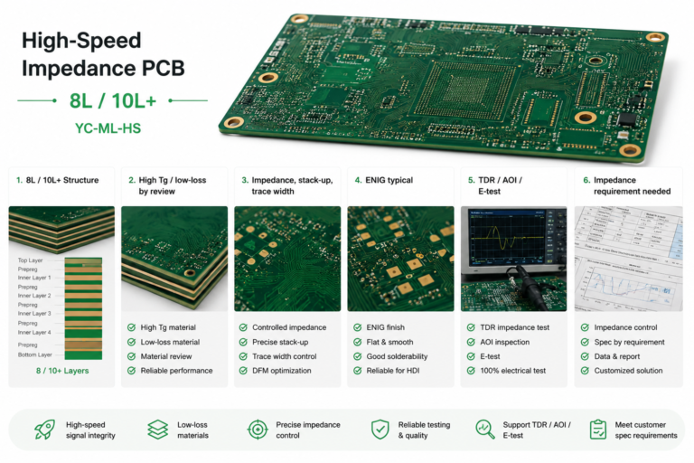
| Impedance targets | Controlled impedance design | Target ohms, tolerance, layers, single-ended or differential |
| Copper weight | Etch and plating | Per layer, outer and inner |
| Surface finish | Assembly compatibility | Named type, lead-free requirement |
| Solder mask and legend | Appearance and function | Colour, spec, any halide restriction |
| Panelisation preference | Cost and assembly | Array, spacing, fiducials, break-away method |
| cURL Too many subrequests by single Worker invocation. To configure this limit, refer to https://developers.cloudflare.com/workers/wrangler/configuration/#limits | What counts as a pass | IPC class, warp limit, cosmetic standard |
Do Not Assume These
- That a quoted layer count equals a capability ceiling. A 32-layer example on a supplier's site is a showcase, not a statement that every 32-layer design is routine.
- That "impedance controlled" is a checkbox. Without a stack-up it is a request, not a specification.
- That hole size in the drill file will be the finished hole size. Plating adds copper; specify whether dimensions are finished or drilled.
- That the fabricator will catch a design error. cURL Too many subrequests by single Worker invocation. To configure this limit, refer to https://developers.cloudflare.com/workers/wrangler/configuration/#limits.
- cURL Too many subrequests by single Worker invocation. To configure this limit, refer to https://developers.cloudflare.com/workers/wrangler/configuration/#limits. cURL Too many subrequests by single Worker invocation. To configure this limit, refer to https://developers.cloudflare.com/workers/wrangler/configuration/#limits.
cURL Too many subrequests by single Worker invocation. To configure this limit, refer to https://developers.cloudflare.com/workers/wrangler/configuration/#limits
cURL Too many subrequests by single Worker invocation. To configure this limit, refer to https://developers.cloudflare.com/workers/wrangler/configuration/#limits. cURL Too many subrequests by single Worker invocation. To configure this limit, refer to https://developers.cloudflare.com/workers/wrangler/configuration/#limits.
cURL Too many subrequests by single Worker invocation. To configure this limit, refer to https://developers.cloudflare.com/workers/wrangler/configuration/#limits. cURL Too many subrequests by single Worker invocation. To configure this limit, refer to https://developers.cloudflare.com/workers/wrangler/configuration/#limits.
cURL Too many subrequests by single Worker invocation. To configure this limit, refer to https://developers.cloudflare.com/workers/wrangler/configuration/#limits. A through-hole via on a thick board is a stub. Above a few GHz, back-drilling or blind vias become part of the design, not an optional extra.
Test point starvation. Dense boards often leave no room for test pads, and then electrical test coverage drops. Reserve test access during layout.
Silkscreen over pads. Cosmetic in fabrication, a solder defect in assembly. Mask and legend rules should be checked against the assembly process.
Design-to-Order Checklist
- Place components first; add layers only after a routing attempt on the minimum stack-up.
- Make the stack-up symmetric in copper and dielectric.
- Classify every via: through, blind, buried, microvia, via-in-pad. Give diameter, depth and fill requirement.
- Set copper weight per layer and confirm the minimum trace/space that weight allows.
- Balance copper, or tell the fabricator where the imbalance is deliberate.
- Provide a full stack-up with dielectric thickness, not a layer count.
- State impedance targets with tolerance and layers, or state explicitly that none are required.
- Reserve test access and confirm the electrical test method.
- Ask for DFM feedback before tooling and read it against the drawing.
- Keep the approved stack-up as the baseline for every repeat order.
FAQ
How do I know if my design really needs 8 layers instead of 6?
Route it on 6 layers first and count what spills. If the spill is a single congested net, it is a placement problem and 8 layers will not fix it. If you cannot keep a continuous reference plane under your high-speed signals or your BGA escape needs two full routing layers, the extra pair is justified.
Does adding layers always increase cost?
No, it can reduce total cost. Two extra layers often remove the need for dense fine-line routing, reduce via count and improve yield on a board that was marginal at a lower layer count. The comparison to run is total cost per good board, not price per square metre at a given layer count.
What is the maximum aspect ratio a fabricator can plate reliably?
Capability varies by factory and by hole size, so ask for the number rather than assuming. The practical discussion starts around 8:1, where hole copper uniformity becomes a real process challenge. Above that, ask how the fabricator verifies barrel thickness — a cross-section per lot, not a promise.
Can I change layer count after the design is finished?
Not without a re-spin. Layer count changes the stack-up, the via structure, the drill program and usually the impedance geometry. It is a new design, not an edit, which is why adding one spare pair early is cheaper than adding two layers late.
Why YC PCB
- 20+ years of multilayer fabrication, with a 6- to 32-layer production route including 16, 20, 30 and 32-layer examples
- HDI capability for high-density BGA fan-out, including a 20-layer FR4 HDI build
- Impedance control with stack-up-based calculation and impedance coupons on request
- DFM/DFA engineering review before release; NDA available for customer IP
- AOI and electrical test on bare boards; X-Ray, ICT and FCT for assembly projects
- ISO 9001 and UL certification; RoHS compliance documentation on request
- No MOQ / No MOV on standard boards, quoted per project for special materials
Get a Quote — Send your Gerber, drill, stack-up and impedance targets with layer count, quantity and target date. Our engineers reply with DFM notes, stack-up confirmation and pricing within one working day.

 French
 English
 Japanese
 German
 Spanish
 Italian
 Portuguese
 Russian
 Dutch
 Turkish
