
Telecom PCB & PCBA Manufacturing
Source bare PCBs and assembled boards for 5G equipment, routers, switches, optical communication modules and network infrastructure. YC PCB supports high-layer-count, HDI, controlled-impedance and high-frequency boards, together with component sourcing, SMT, THT and BGA assembly, inspection and project-specific testing.
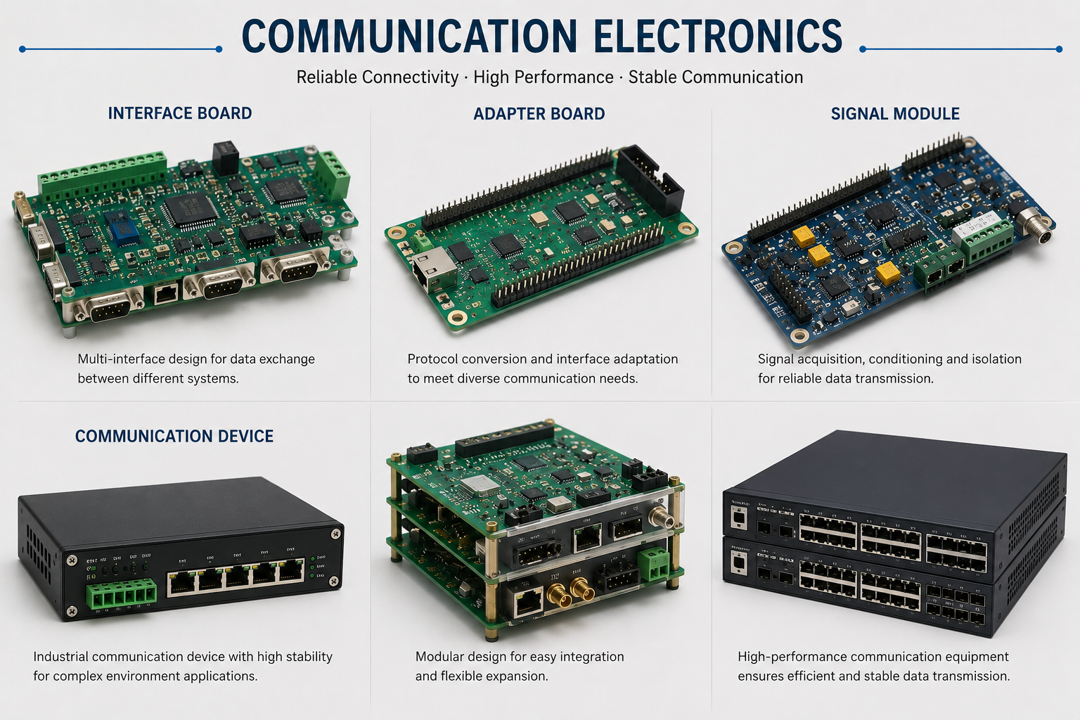
Years PCB and PCBA manufacturing experience
High-layer-count manufacturing capability up to 40 layers
Blind and buried vias, microvias and dense BGA routing support
Component sourcing, SMT, THT, BGA, inspection and testing
Reliable PCBs for High-Speed Network Equipment
Telecom buyers need boards that preserve signal integrity, handle continuous thermal load, maintain connector reliability and repeat consistently from prototype to batch production. YC PCB confirms the complete manufacturing route before quotation so material, stack-up, via structure, surface finish and testing align with the final equipment.
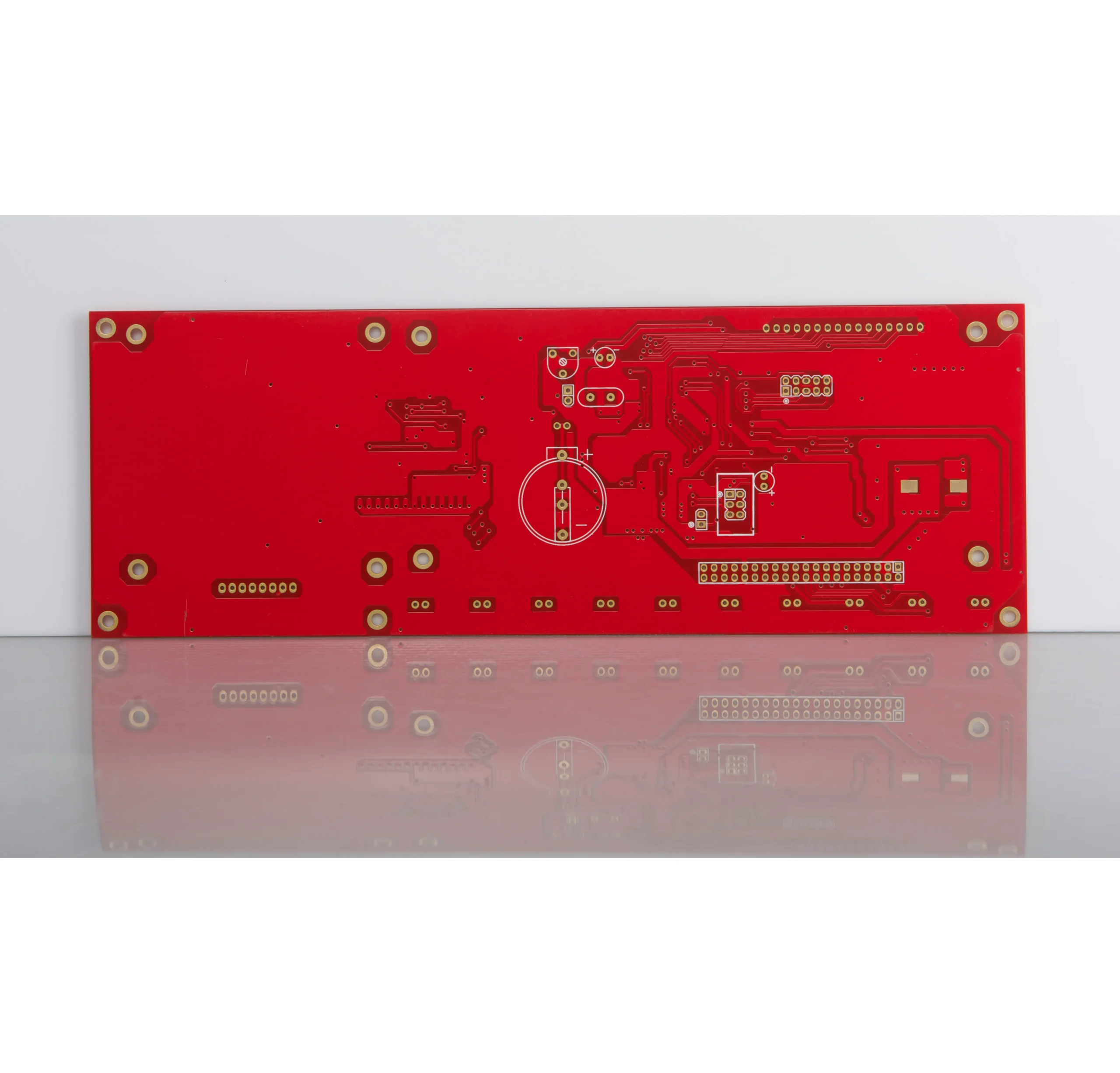
Engineering Review Before Production
Send your stack-up, impedance table, connector details and operating requirements so the manufacturing and test route can be confirmed before pricing.
PCB Options for Telecom and Network Equipment
Select the PCB route according to signal speed, operating frequency, layer count, connector design, thermal load and assembly scope. YC PCB supports bare board and turnkey PCBA orders from prototype through repeat production.
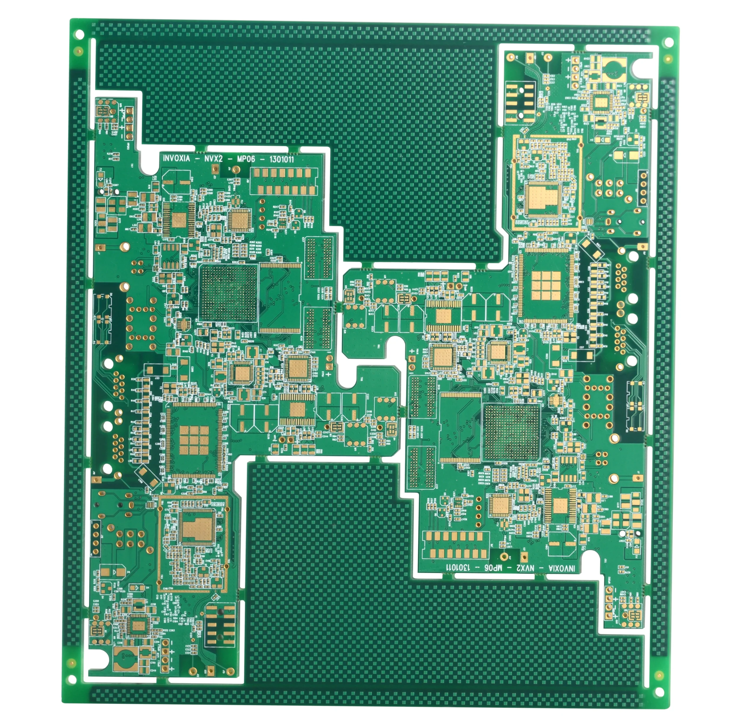
5G PCB
Multilayer and controlled-impedance boards for base station modules, radio control, signal processing and high-speed communication designs.
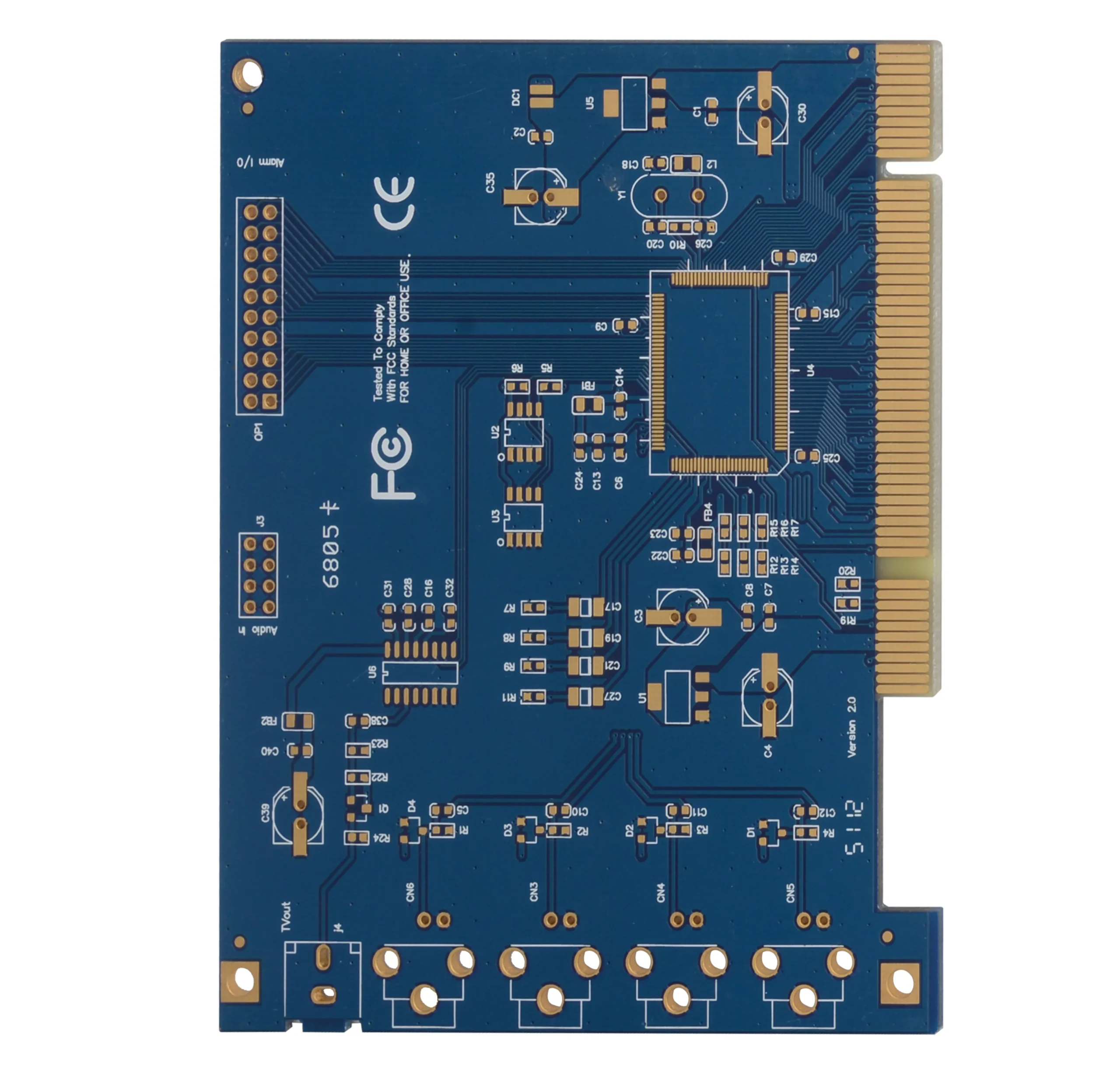
Network Equipment Board
High-layer-count and connector-intensive boards for routers, switches, gateways, server interfaces and other network equipment.
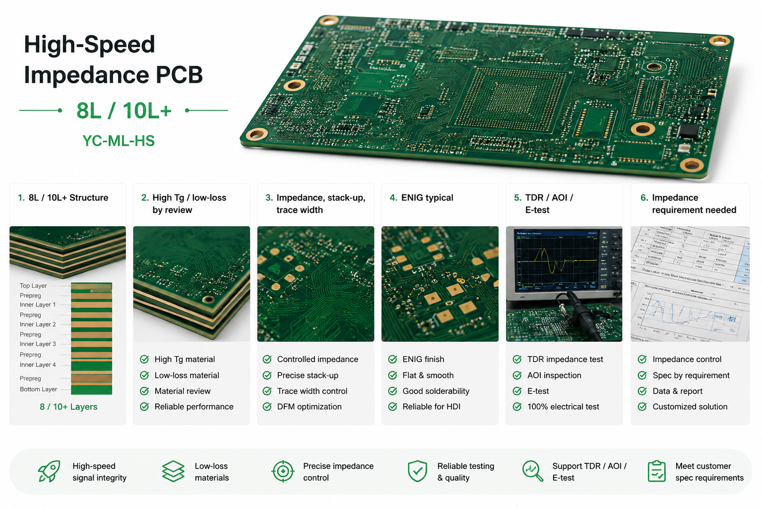
High-Frequency PCB
Low-loss material and impedance-controlled routes for RF modules, antennas, transceivers and signal-sensitive communication hardware.

HDI Telecom PCB
Blind and buried vias, microvias and via-in-pad options for compact BGA layouts and high-pin-count telecom electronics.

Thermal Management Board
Copper balance, power-plane and heat-spreading support for continuously operating communication and power modules.
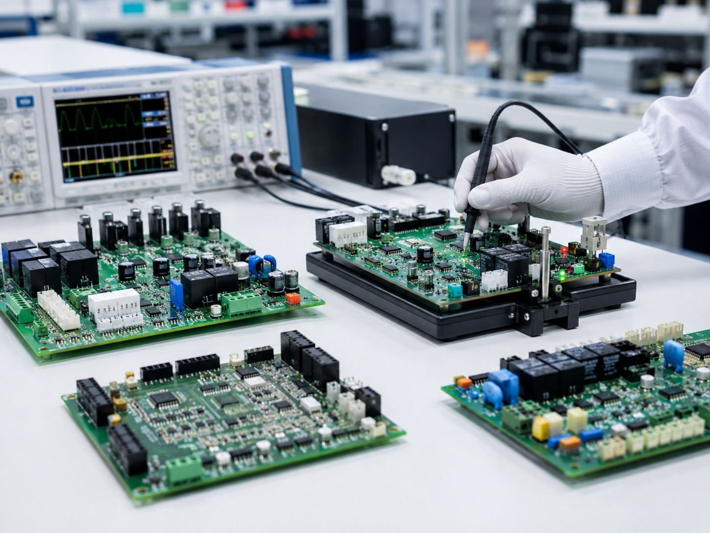
Telecommunications PCBA
Component sourcing, SMT, THT and BGA assembly, AOI, X-Ray, ICT, FCT and programming for finished communication assemblies.
Key Controls for Telecom PCB Reliability
A telecom PCB is only as reliable as its material, stack-up, interconnect, connector and inspection controls. These manufacturing decisions should be confirmed before the first build.
Controlled Impedance
We confirm target values, reference layers, dielectric thickness, trace geometry and coupon requirements for single-ended and differential signals.
Material Selection
FR4, high-Tg, high-frequency and low-loss materials are selected according to channel length, operating frequency, thermal environment and cost target.
BGA and Via Structure
BGA fanout, via-in-pad, blind and buried vias, microvias, drill limits and layer registration are checked for manufacturability.
Thermal Reliability
Copper distribution, power planes, heat concentrations and assembly temperatures are reviewed for continuous network operation.
Connector Durability
Gold fingers, edge connectors, press-fit areas, connector tolerances and wear requirements are checked against mechanical use.
PCBA Inspection
AOI, X-Ray, electrical test, ICT, FCT, programming and communication tests are selected according to the finished product.
From Engineering Files to Tested Telecom PCBA
A coordinated manufacturing route helps reduce design revisions, avoid assembly delays and maintain repeatability from prototype to batch production.
Engineering File Review
Gerber, drill, stack-up, impedance, material, BGA, connector and assembly requirements are checked before quotation.
Material & Stack-Up Confirmation
Base material, dielectric thickness, copper weight, signal layers and power-plane arrangement are confirmed before production.
PCB Manufacturing
Multilayer, HDI, high-frequency and controlled-impedance boards are manufactured according to the approved specification.
Surface Finish & Connector Plating
ENIG, immersion gold, gold fingers or other finishes are selected according to solderability, storage and connector wear requirements.
Component Sourcing & Assembly
Components are sourced and assembled through SMT, THT, BGA, QFN, connector and mixed-assembly processes as required.
Inspection, Test & Delivery
AOI, X-Ray, electrical testing, ICT, FCT, programming and packing checks are completed according to the agreed test scope.
Telecom and Network Equipment Applications
YC PCB supplies bare boards and assembled PCBA for communication hardware that requires high-speed routing, dense interfaces, reliable assembly and defined testing.
5G Base Stations
Multilayer, high-frequency and controlled-impedance boards for radio control, communication and power-distribution modules.
Routers & Switches
Connector-intensive multilayer boards for routers and switches with dense ports and high-speed signal channels.
Server Hardware
High-layer-count backplanes, control boards and interface boards for server and network infrastructure.
Optical Communication
Compact high-speed boards for optical modules, transceivers and signal-conversion hardware.
RF Modules
Low-loss and impedance-controlled boards for radio-frequency modules and signal-sensitive circuits.
IoT Gateways
Compact PCBA combining RF, digital control, power management and connectivity functions.
Communication Power
Power-supply, converter and thermal-control boards for continuously operating telecom equipment.
Data Center Equipment
High-speed boards and PCBA for servers, switches, storage systems and data-center infrastructure.
Information Needed for an Accurate Telecom PCB Quote
Providing complete files allows YC PCB to confirm feasibility, material, process, test scope, lead time and pricing without repeated clarification.
| Project Item | Review Scope | Information to Provide |
|---|---|---|
| PCB Type | Multilayer PCB, HDI PCB, high-frequency PCB, rigid-flex PCB, impedance control PCB, telecommunications PCBA | Application, product function, layer count and board outline |
| Signal Requirement | High-speed routing, differential pairs, controlled impedance, reference plane and return path review | Stack-up, impedance table, trace notes and key net information |
| Material Route | FR4, high Tg FR4, high-frequency material, ENIG / immersion gold / gold finger options | Material brand if required, Dk/Df notes, Tg requirement and surface finish |
| Interconnect Design | BGA fanout, blind / buried via, via-in-pad, connector area and edge connector review | BGA pitch, via type, connector drawing and mechanical fit notes |
| PCBA Route | SMT, BGA, QFN, THT connectors, component sourcing, programming and test route | BOM, pick-and-place file, assembly drawing and programming notes |
| Inspection Route | AOI, X-Ray, electrical test, ICT, FCT or project-based communication test | Test method, test points, fixture requirement and acceptance standard |
Prepare Your Telecom PCB or PCBA RFQ
Send the following information for a manufacturing route, lead-time and quotation review.
Send Your Telecom PCB Requirements
Submit your contact details and project requirements through our quick inquiry form. For Gerber files, ODB++, stack-up, impedance tables, BOM, drawings or other attachments, email them directly to our engineering team.
Email: sales@ycelectronic.com
Telecom PCB & PCBA FAQ
Answers to common sourcing and engineering questions for telecom PCB, 5G PCB and network-equipment PCBA projects.
What is a telecom PCB?
A telecom PCB is a circuit board manufactured for communication equipment such as routers, switches, base stations, optical modules, servers and network-control systems.
What makes a 5G PCB different from a normal PCB?
5G boards often combine controlled impedance, low-loss or high-frequency materials, multilayer or HDI routing, dense interconnects, thermal load and continuous-duty requirements.
What files should I send for a telecommunication PCB quote?
Send Gerber files, drill file, stack-up, impedance table, material notes, surface finish, quantity and delivery target. If assembly is needed, also send BOM, pick-and-place file and assembly drawing.
Can YC PCB support telecommunications PCBA?
Yes. Services can include PCB fabrication, component sourcing, SMT, THT, BGA and QFN assembly, AOI, X-Ray, electrical testing, ICT, FCT and programming according to project requirements.
Do telecom PCBs need impedance control?
Many telecom boards need controlled impedance because high-speed signals are sensitive to layer structure, dielectric thickness, copper thickness and trace geometry.
Can flexible PCB be used in telecom equipment?
Yes. Flexible PCB and rigid-flex PCB can be used for compact interconnects, space-constrained modules and designs that need fewer connectors or improved vibration resistance.
Which surface finish is suitable for communication circuit boards?
ENIG, immersion gold, gold fingers and other finishes are selected according to solderability, storage time, connector wear and assembly requirements.
Can you test the finished telecom PCBA?
Testing can include AOI, X-Ray, electrical test, ICT, FCT, programming or project-specific functional test based on the product and test fixture availability.
Send Gerber, Stack-Up, Impedance and PCBA Files
Receive a quotation based on your actual layer count, material, signal, connector, assembly, testing and delivery requirements.
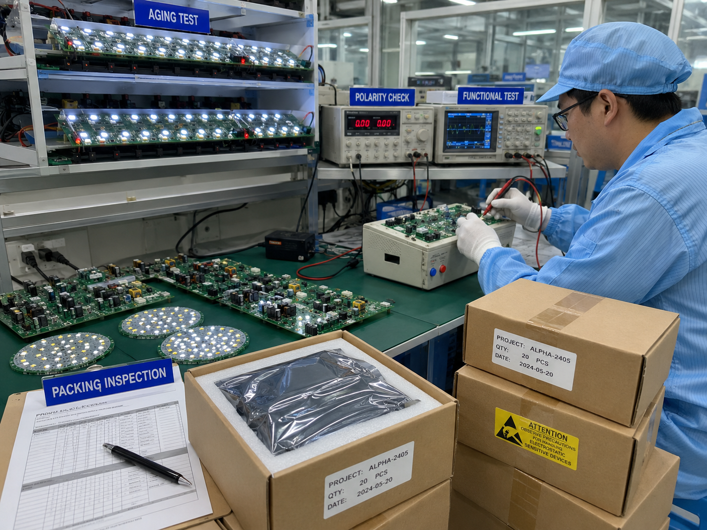
One Manufacturing Route for PCB and PCBA
Coordinate PCB fabrication, component sourcing, SMT, THT and BGA assembly, inspection, testing and shipment through one manufacturing workflow.
Send Your PCB Requirements
Tell us what you need. For Gerber files, ODB++, stack-up, impedance tables, BOM, drawings or other attachments, email them directly to sales@ycelectronic.com after submitting this form.
 English
  Japanese
  French
  German
  Spanish
  Italian
  Portuguese
  Russian
  Dutch
Dutch  Turkish