 Skip to content
Leading PCB Manufacturer for Global Electronics Brands
Custom PCB Solutions | Fast Turnaround | Quality Guaranteed | 20+ Years Experience
Why 10,000+ Electronics Brands Trust Us
Our Competitive Advantages in PCB Manufacturing
Experience & Scale
20+ years industry experience, 300+ employees, 4,000 m²/day production capacity
Full Product Coverage
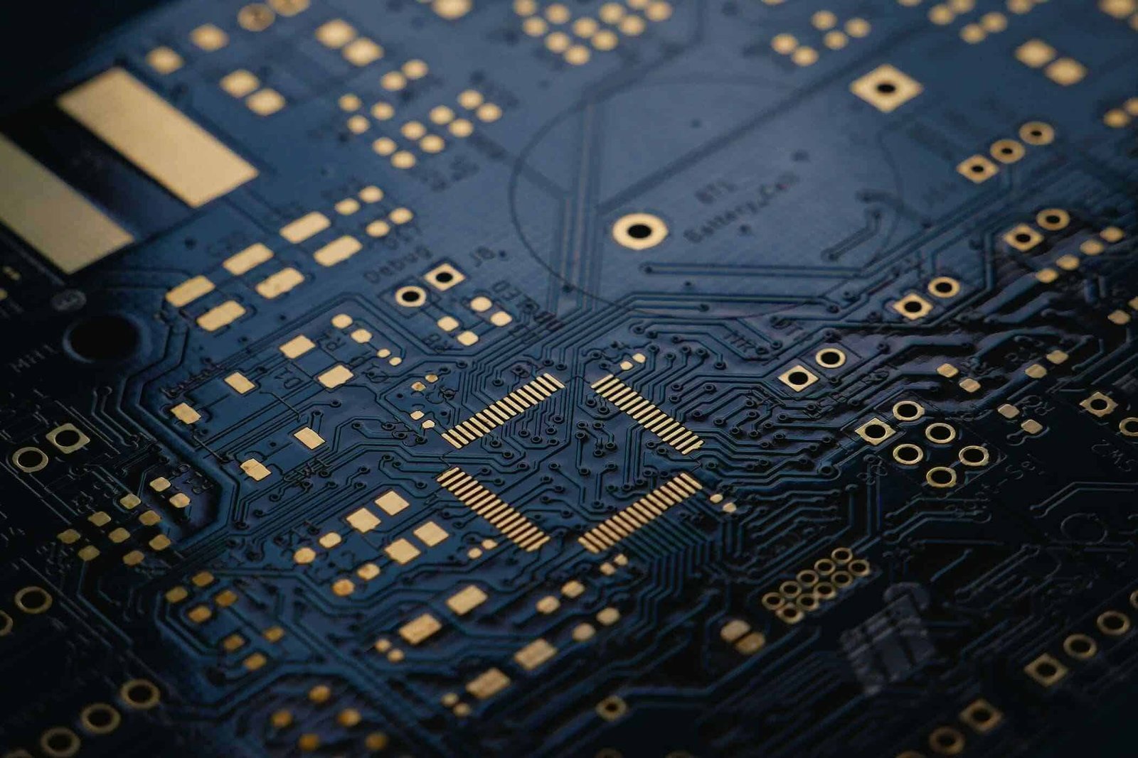
Single/Double/Multilayer, HDI, Flexible, Rigid-Flex, Aluminum, RF PCB
Fast Sampling & Quality
1-3 days samples, 99.5% quality rate, ISO 9001 & IPC-A-600 certified
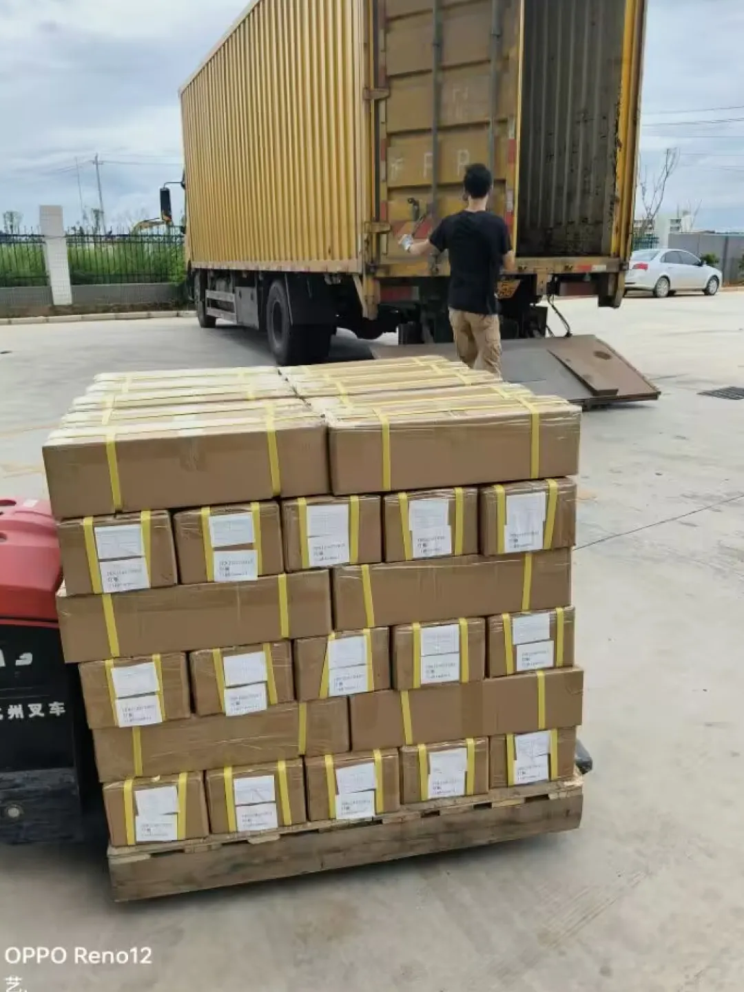
Global Logistics
Express & standard shipping to 60+ countries, professional packaging

24/7 Technical Support
Dedicated engineers, multi-language support, quick response time
About YC PCB | Trusted PCB Manufacturer Since 2003
Serving the Global Electronics Industry with Quality & Innovation

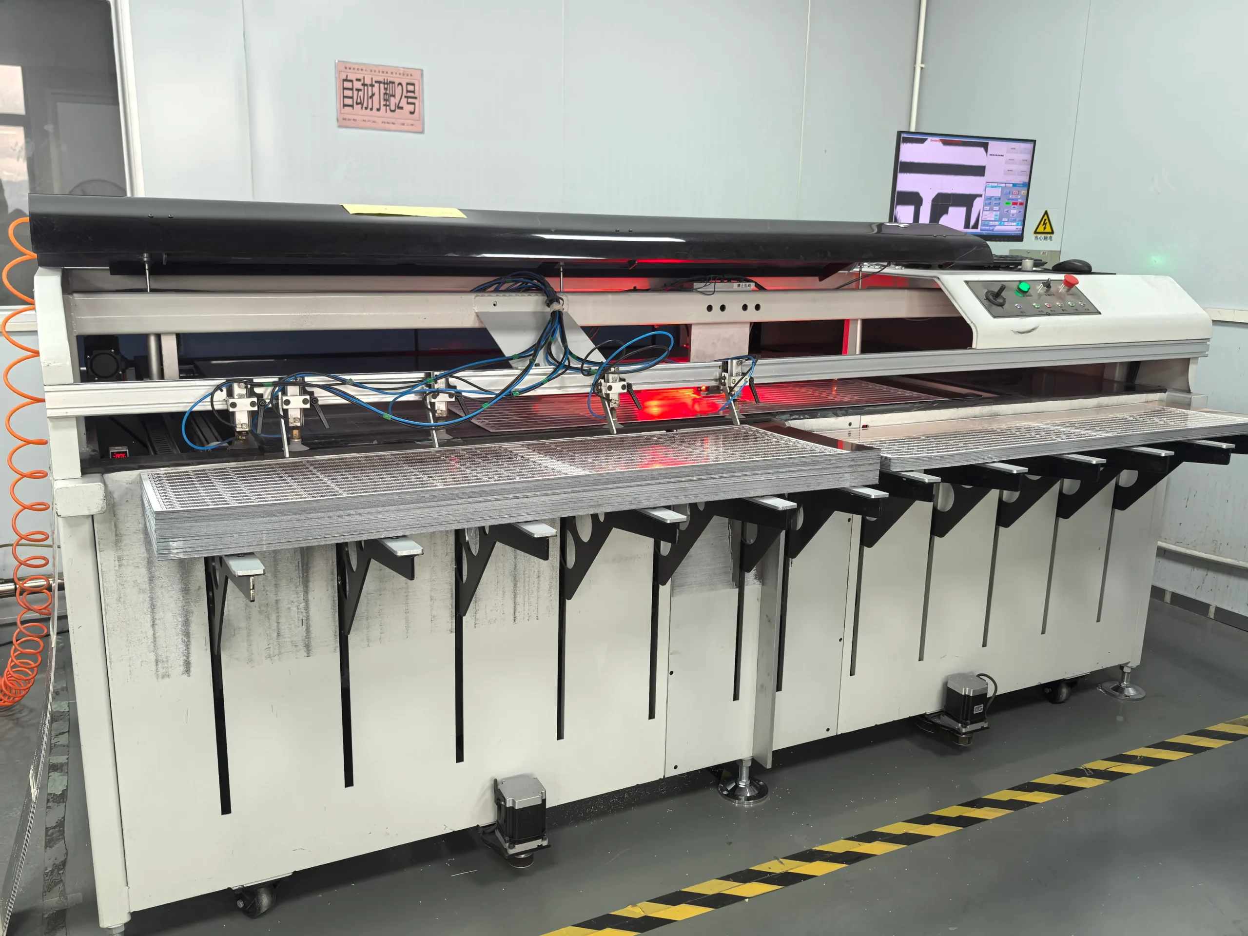
Founded in 2003, YC PCB has grown to become one of China's leading PCB manufacturers. With a commitment to quality and innovation, we have earned the trust of electronics brands worldwide.
Professional Employees
Production Lines
Daily Capacity
Countries Served
Our facility spans 20,000 sq.m with state-of-the-art equipment for PCB manufacturing and PCBA assembly. We specialize in custom PCB solutions across automotive, consumer electronics, telecommunications, industrial, and medical industries.
Our Commitment: Quality First, Customer Success, Innovation Always. Every PCB undergoes rigorous inspection to ensure zero-defect delivery.
Global Customers
Quality Rate
Years Experience
Traceability
Full Range of PCB Solutions We Offer
From Standard PCB to Advanced HDI, Flexible, and Specialty Boards
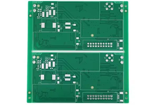
Standard PCB
Cost-effective single and double-layer boards for basic applications

Multilayer PCB
4 to 20 layers with impedance control for complex circuits
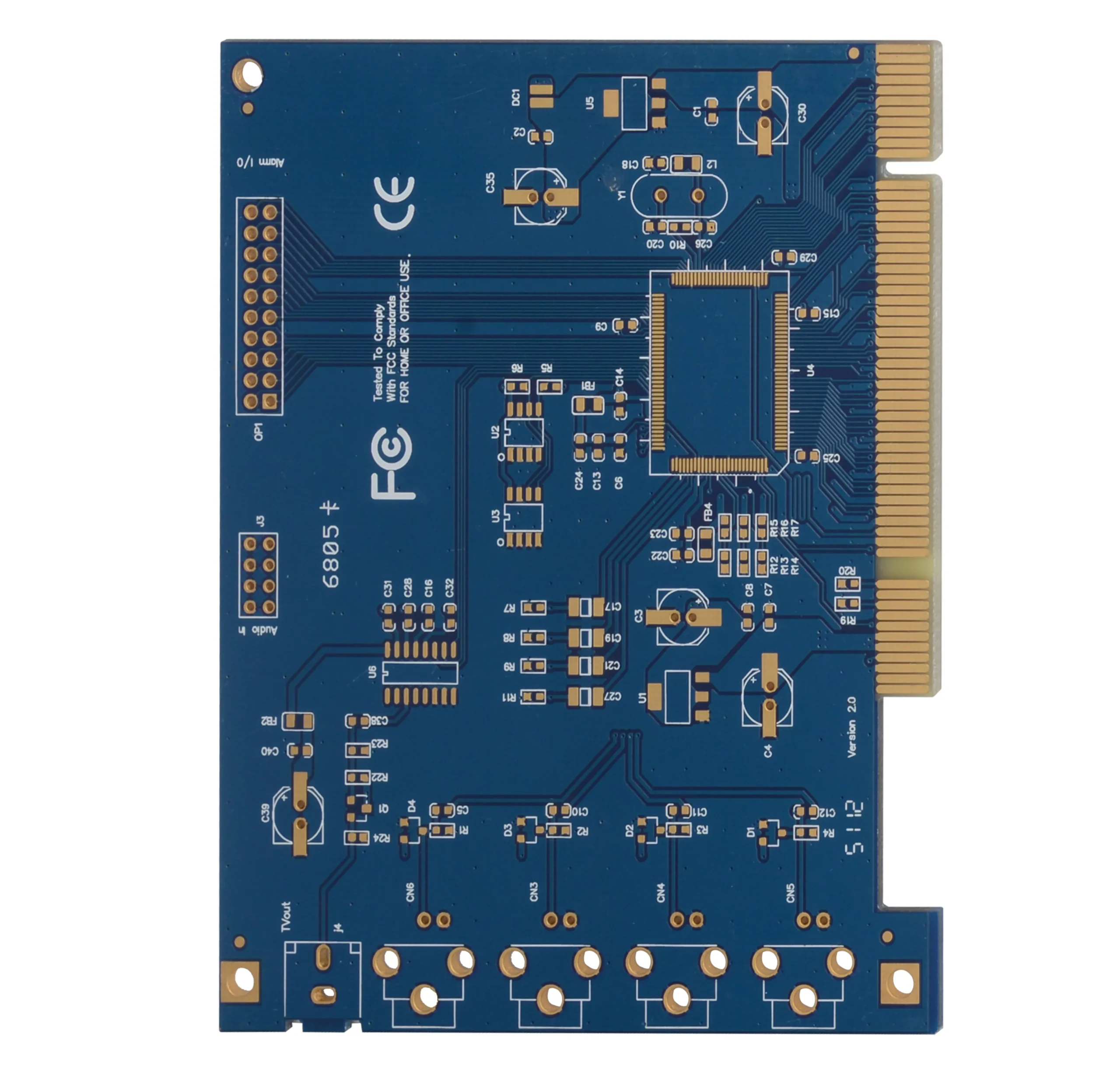
HDI PCB
High-density interconnect with micro vias for advanced devices
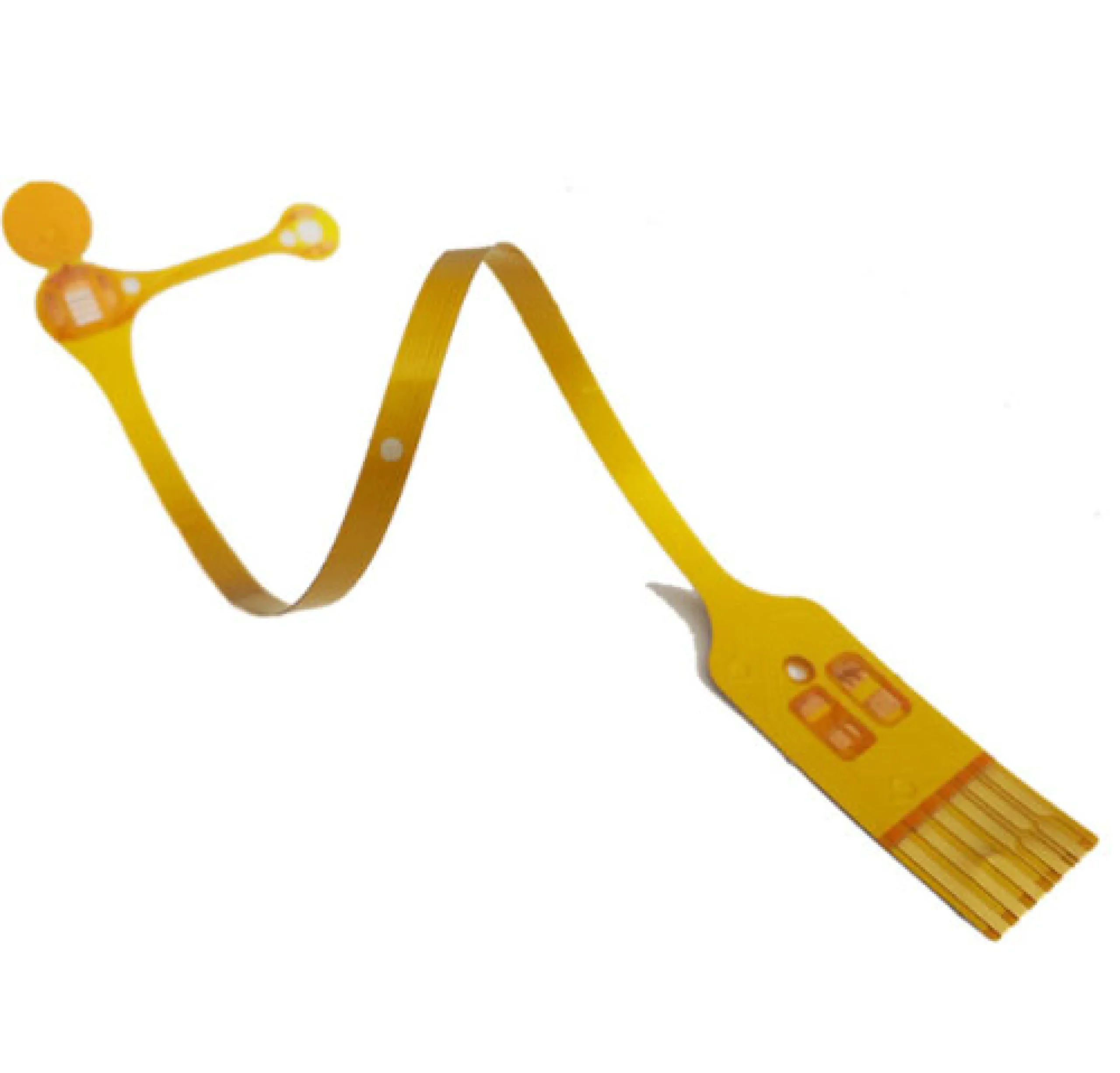
Flexible PCB
Polyimide-based flexible boards for foldable and space-saving designs
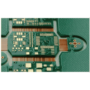
Rigid-Flex PCB
Hybrid rigid and flex sections for complex 3D applications

Aluminum PCB
Excellent heat dissipation for LED drivers and power management
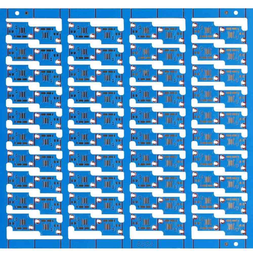

Copper base PCB
Superior heat dissipation, in high-power applications
Don't see what you need? We offer custom solutions for specialized requirements.
Industries We Serve
PCB Solutions for Diverse Market Segments & Applications
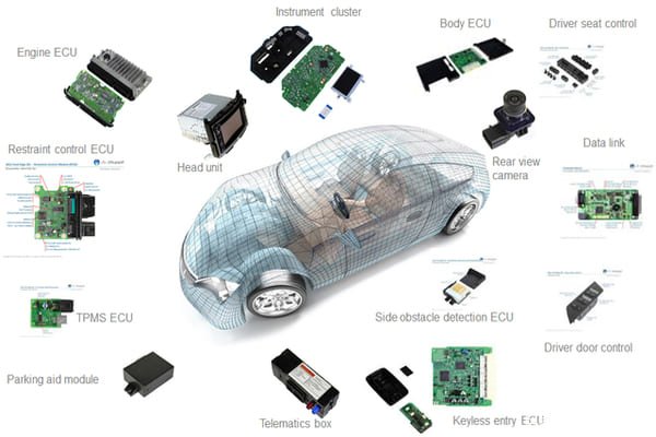
Automotive
ECU, infotainment systems, safety controls, power management modules
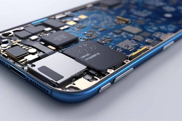
Consumer Electronics
Smartphones, tablets, wearables, smart home devices, gaming

Industrial Equipment
Control systems, VFD drives, PLCs, industrial IoT, robotics
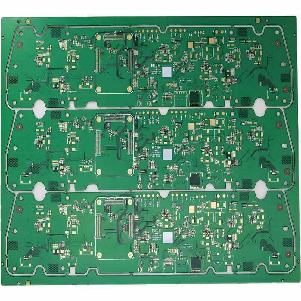
Telecommunications
5G base stations, routers, optical modules, network equipment

Medical Devices
Diagnostic equipment, patient monitors, implants, healthcare IoT
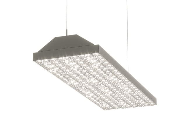
LED & Lighting
LED drivers, power supplies, smart lighting, street lights, tubes
Need a solution for your industry? Our engineers can help design the perfect PCB for your application.
Contact Our Technical Team →Manufacturing Excellence
State-of-the-Art Manufacturing Facility
Advanced Equipment & Technology for Quality PCB Production
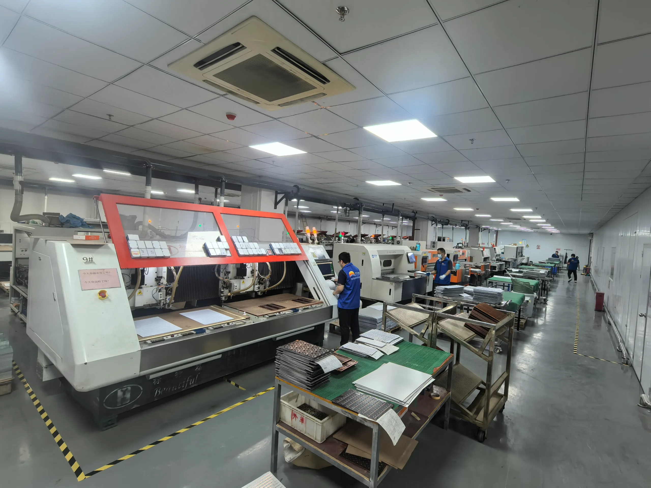
20,000 sq.m Production Area
15+ Production Lines | 4,000 m²/day Capacity

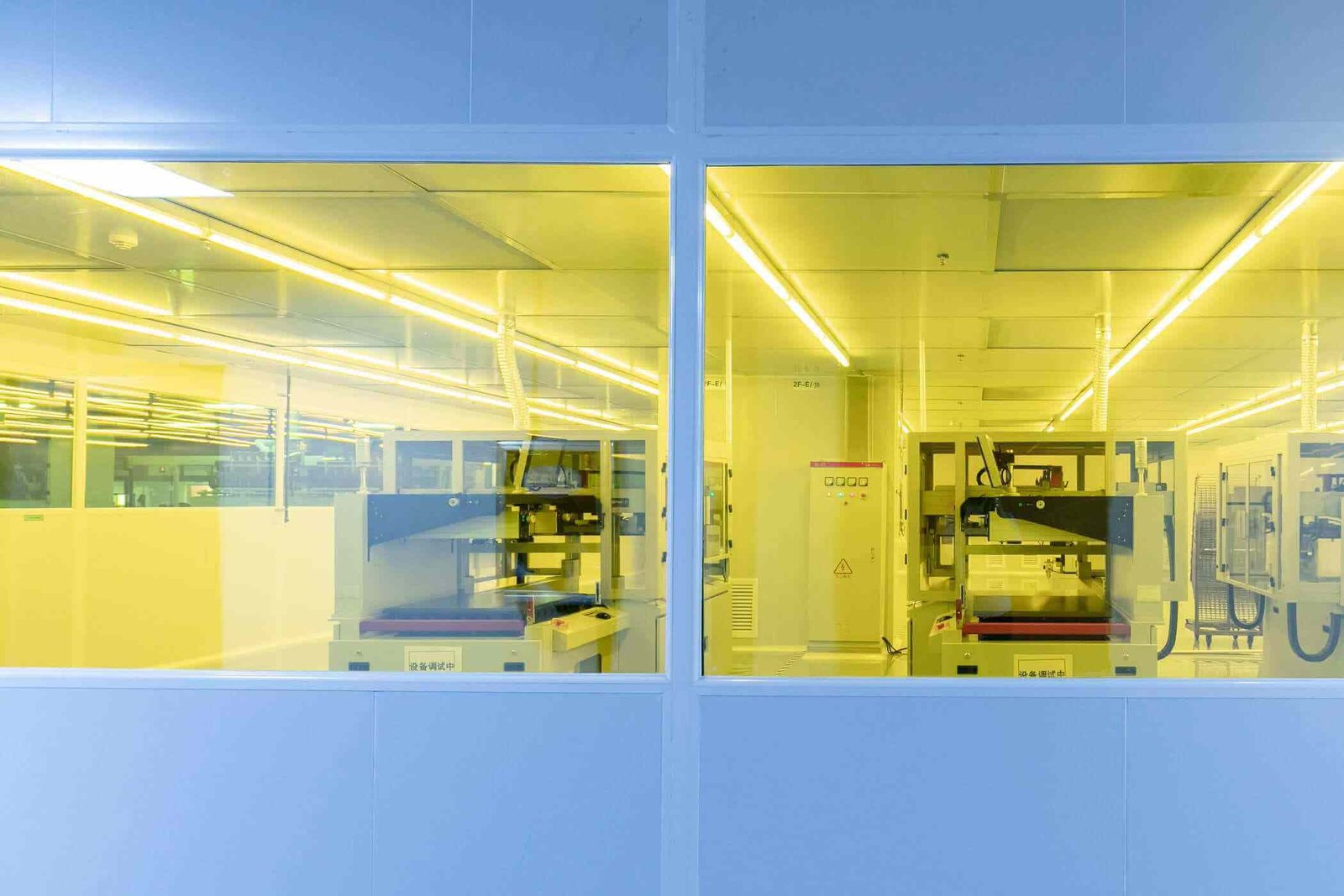
Clean Room Standard
Automated & Semi-Automated Lines | ISO Certified
Key Manufacturing Equipment
Lamination Press
Multi-layer Lamination | Pressure Control | Precision Heat
Etching Equipment
Chemical Etching | High Precision | Environmental Control
CNC Drilling
Multi-spindle Drilling | 0.1mm Hole | High Speed
Screen Printing
Automated Printing | Multi-Color | Precision Registration
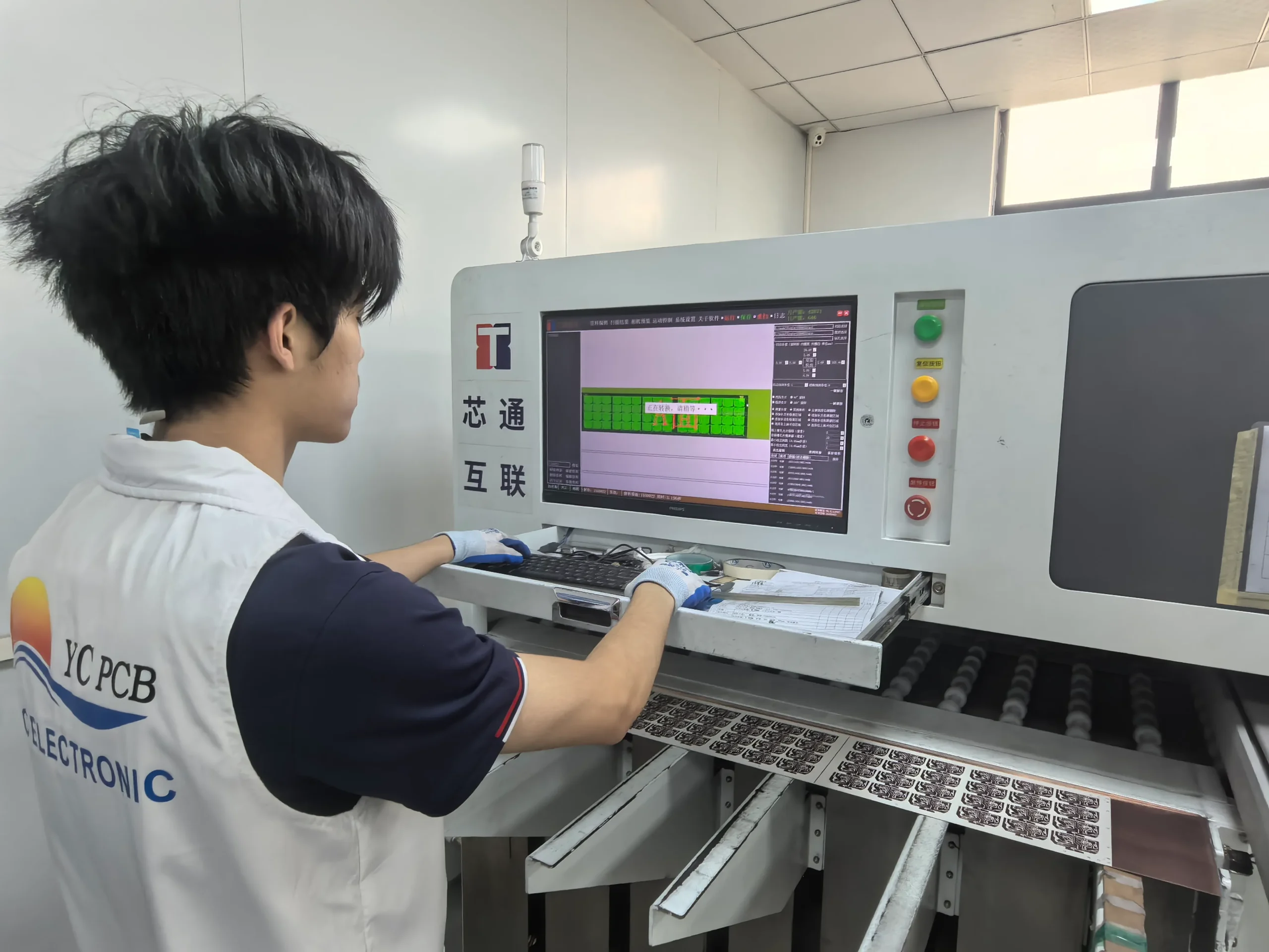
AOI Inspection
100% Optical Inspection | Defect Detection
Electrical Testing
Flying Probe Tester | 100% Coverage | Data Logging
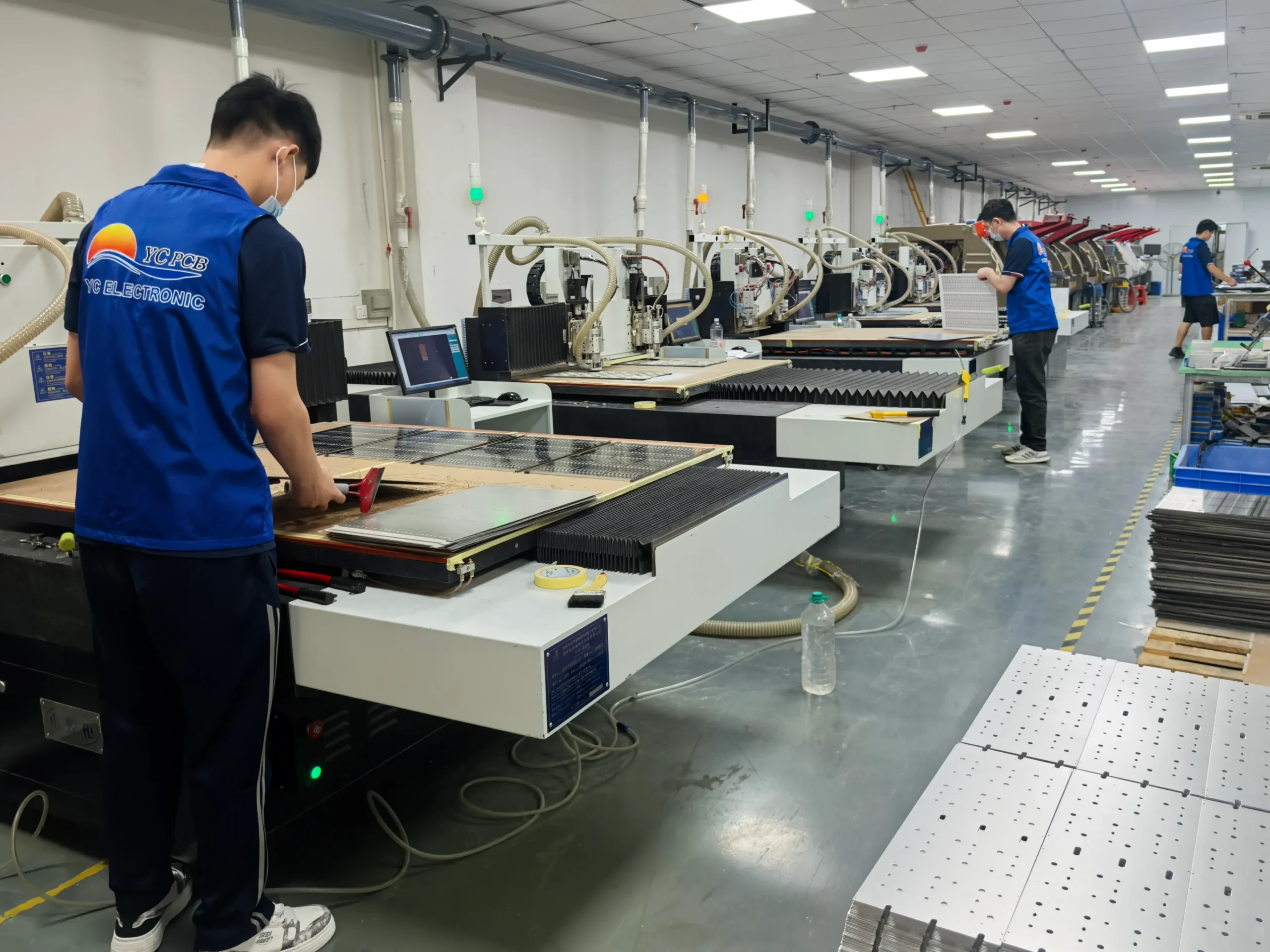
CNC Routing
Precision Cutting | V-Cut Support | Clean Edges
Packaging Equipment
Vacuum Packing | Moisture Control | Labeling

4,000
m²/day Production Capacity
15+
Production Lines
99.5%
First-Pass Quality Rate
24/7
Production Operation
Manufacturing Excellence
Our Manufacturing Process
From Design to Delivery - 12+ Steps to Excellence
Design Review
File Check | DFM Analysis
Material Prep
Quality Selection
Lamination
Heat Press | Layer Bond
Drilling
Precision 0.1mm Holes
Plating
Copper Electroplate
Etching
Pattern Trace Etch
Solder Mask
Green/Blue/Red Apply
Inspection
AOI + E-Test 100%
Routing
CNC V-Cut Depanel
Cleaning
Surface Clean
Quality Check
Final Inspection
Shipment
Fast Logistics
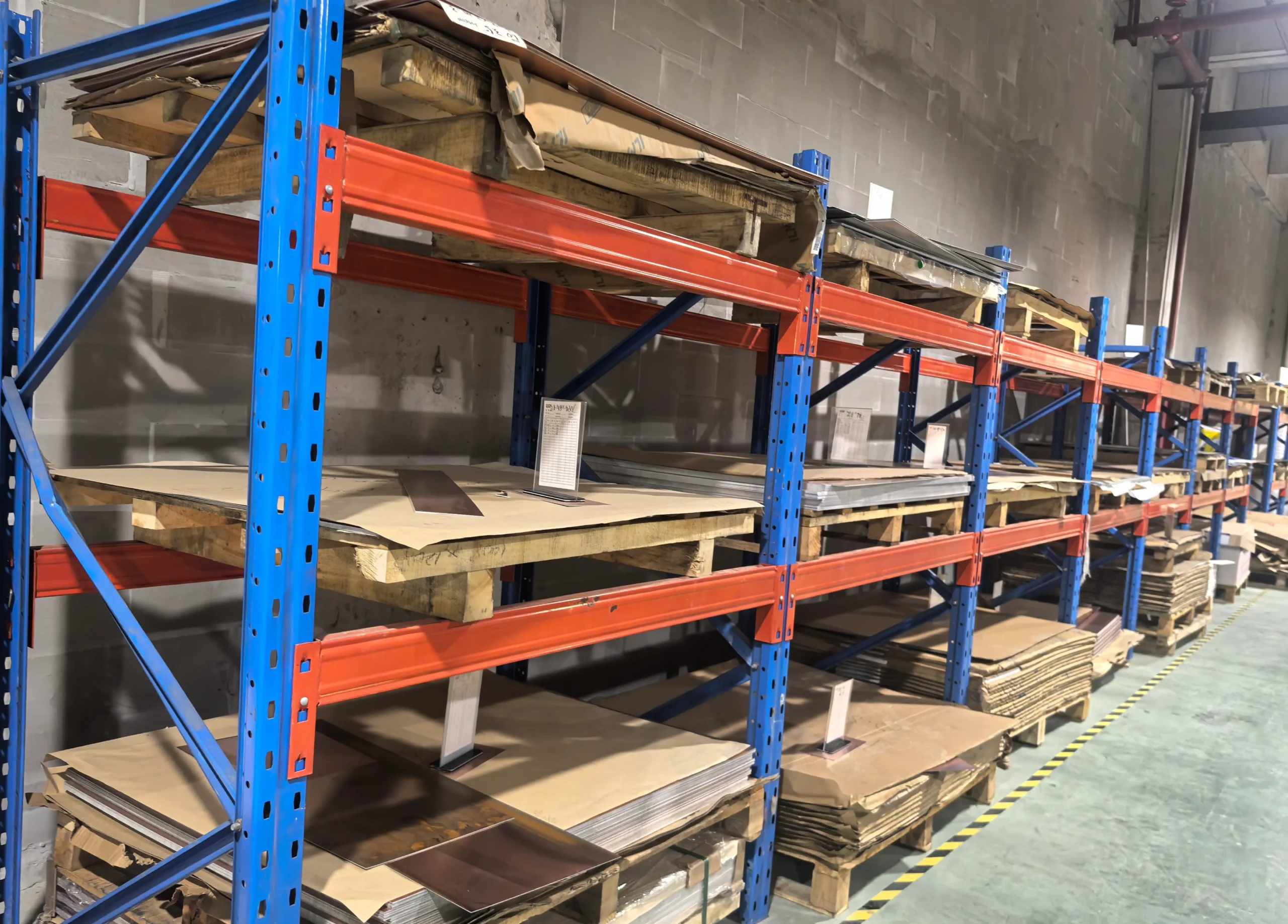
Material Selection & Verification
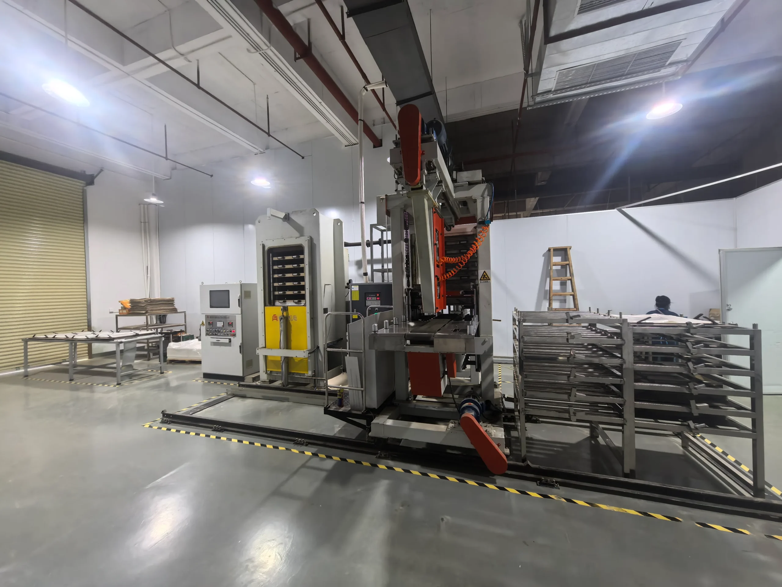
Multi-layer Lamination Process

Chemical Etching & Patterning

Solder Mask & Silkscreen
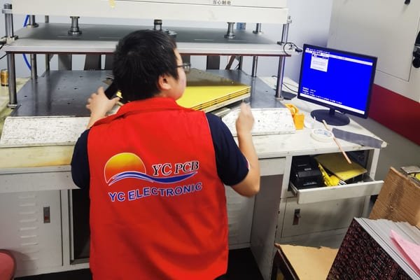
100% Electrical Testing

Packaging & Logistics
Quality Excellence
Quality Assurance & Testing Standards
100% Inspection & Validation for Zero-Defect Delivery
Our Quality Commitment
Every PCB undergoes comprehensive 100% inspection at 5+ critical stages from raw material verification through final shipment. We combine automated optical inspection (AOI), electrical testing (E-Test), and manual quality checks to ensure zero-defect delivery and complete traceability for every order.
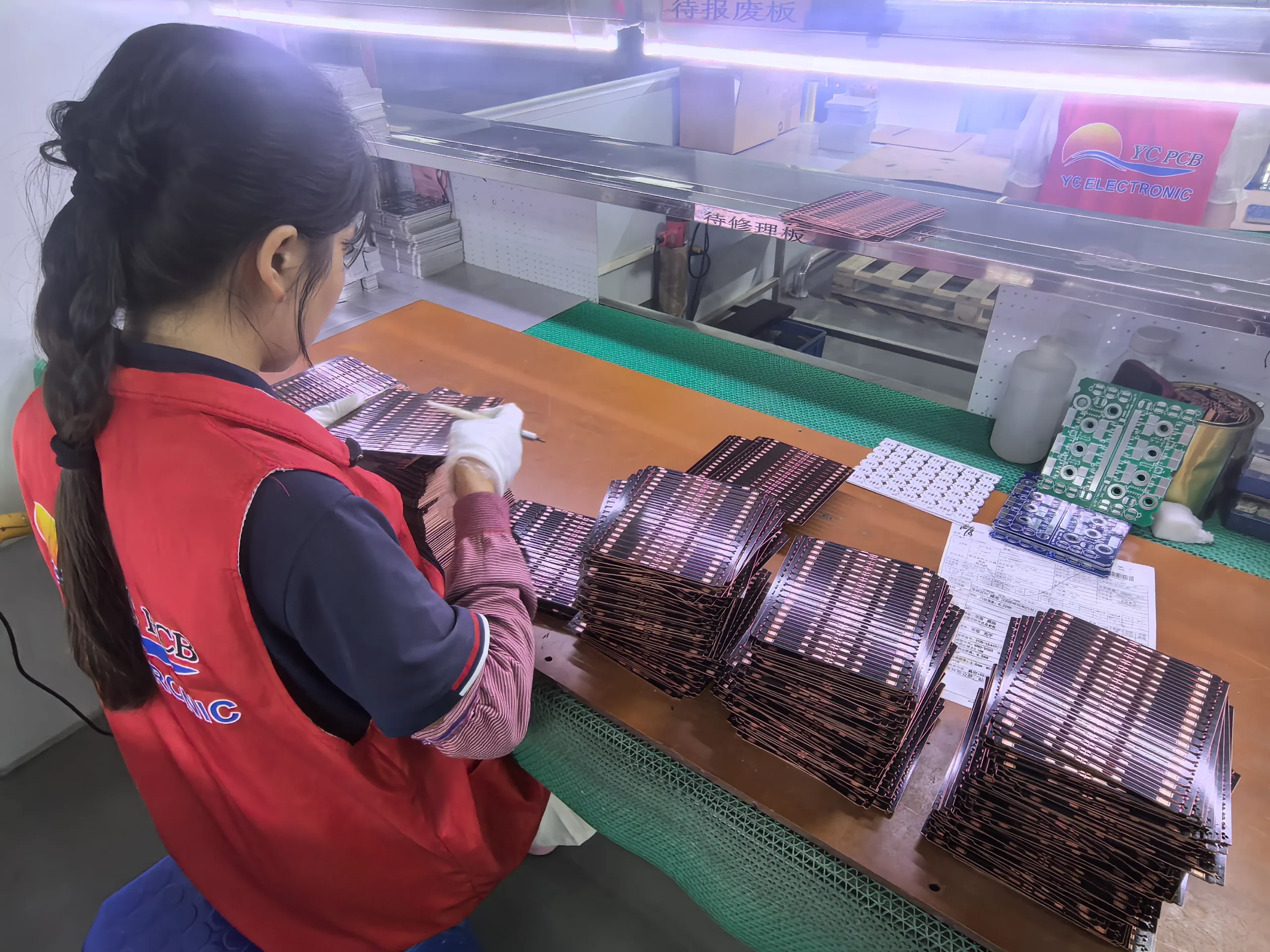
Quality Control Department
Professional Testing Team | Real-time Monitoring | Advanced Equipment
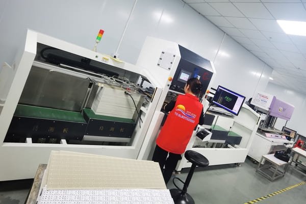
Electrical Testing
Flying Probe Tester | Continuity Check | Short Circuit Detection
5+ Inspection Stages
Incoming Inspection
Raw Materials | Component Verification | Quality Certification
In-Process Inspection
Self-Check | Professional Check | Each Production Stage
Final Inspection
100% AOI | 100% E-Test | Defect Detection
Environmental Testing
Temperature Cycling | Humidity Control | Reliability Validation
Documentation
Inspection Certificate | Test Reports | Full Traceability
Advanced Testing Equipment
AOI System
100% Optical Coverage | Defect Detection | High Accuracy
E-Test (Flying Probe)
Electrical Continuity | Short Circuit Test | No Fixture Required
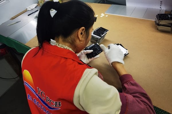
Precision Measurement
Board Thickness | Layer Spacing | Micro Precision
99.5%
First-Pass Quality Rate
Industry-leading performance
<0.3%
Defect Rate
Zero-defect target
100%
Traceability
Full batch tracking
Professional Credentials
Certifications & Industry Standards
Trusted by Global Brands - Certified Excellence
ISO 9001:2015
Quality Management System
IPC-A-600
PCB Acceptability Standards
RoHS 2.0
Hazardous Substance Compliance
IPC-600
Electrical Performance Standards
UL Listed
Safety & Performance
IATF 16949
Automotive Quality Standard
ISO 14001
Environmental Management
ISO 45001
Occupational Health & Safety
Industry Standards Compliance
✓ PCB Manufacturing Standards
- • IPC-A-600: PCB Acceptability Standards
- • IPC-600: Electronic Assemblies
- • IPC-2581: PCB Electrical and Mechanical Data Format
- • IPC-6011: Laminate for Use as Electrical Insulation
- • IPC-6012: Printed Boards
✓ Environmental & Safety Standards
- • RoHS 2.0 (Directive 2011/65/EU)
- • REACH Compliance (Regulation (EC) No. 1907/2006)
- • WEEE Compliance (Directive 2012/19/EU)
- • UL 94 Flammability Standards
- • Lead-Free Manufacturing Capability
All certifications and test reports available upon request. We maintain full compliance with international standards for electronics manufacturing.
Our Valued Partners
Long-Term Cooperation With Trusted Brands
Real partnerships are built through repeat orders, engineering trust, and dependable delivery.


24 Hours Service
Real Customer Chat Records


98% Customers Would Repeat Purchase


Reliable Shipment & Global Logistics
Professional packaging and worldwide delivery to ensure your PCBs arrive in perfect condition
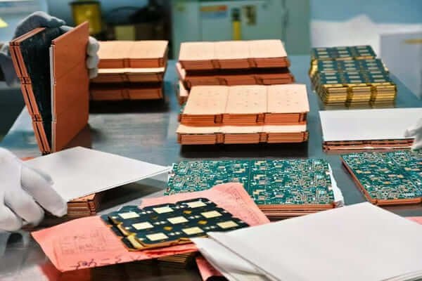
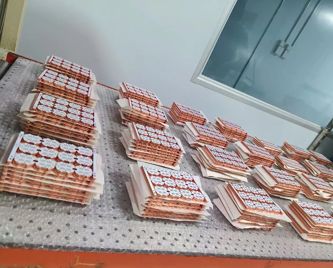
Professional Packaging Standards
Vacuum Sealed Packaging
Multi-layer vacuum bags with moisture-absorbing desiccant for protection against humidity and contamination
Static-Safe Handling
ESD-compliant packaging to prevent electrostatic discharge damage during transport and storage
Reinforced Box & Padding
Heavy-duty corrugated boxes with foam inserts and protective wrapping for maximum impact resistance
Complete Labeling & Documentation
Inspection certificates, packing lists, batch numbers, and QC reports included in every shipment
From Factory Floor to Your Doorstep
1. Final QC Check
100% inspection verified before packing

2. Vacuum Sealing
Protected with desiccant for moisture control
3. Box Packing
Reinforced boxes with protective cushioning

4. Fast Dispatch
Expedited logistics to 60+ countries
Global Logistics Partners
DHL Express
Fast worldwide shipping
FedEx International
Reliable courier service
UPS
Global tracking & insurance
Local Carriers
Cost-effective options
Our Shipping Commitment
- → Real-time Tracking - Know exactly where your PCBs are
- → Insurance Included - Full coverage for peace of mind
- → Fast & Flexible - Express, Standard, or Sea freight options
Unlimited Customization Possibilities
We handle your most challenging requirements with advanced engineering and flexible manufacturing
Advanced Materials
- • FR-4 & FR-4 High Tg - Standard to high-temperature
- • Polyimide (PI) - For flexible & high-temp applications
- • Rogers, Teflon (PTFE) - RF & microwave boards
- • Aluminum & Copper Clad - Thermal management
- • Custom Prepreg & Resin - Special formulations
Precision Process Control
- • Impedance Matching - ±10% accuracy for high-speed
- • Thickness Control - 0.4mm to 12mm+ options
- • Line Width & Spacing - Down to 0.1mm traces
- • Copper Weight - ½oz to 4oz per layer
- • Via & Hole Sizing - Micro vias (0.1mm) to large holes
Special Processes
- • Blind & Buried Vias - Complex multilayer designs
- • Plated Half-Holes - Edge connector applications
- • Selective Plating - Gold, silver, nickel finishes
- • HDI & Microvias - 0.05mm vias for ultra-dense boards
- • Laser Drilling & Ablation - Precision micro-features
Surface Finishes
- • HASL / Lead-free HASL - Cost-effective standard
- • ENIG / Immersion Gold - Fine-pitch components
- • OSP / Organic Coating - Environmentally friendly
- • Hard Gold Plating - Connector & high-wear areas
- • Selective Plating - Multiple finishes on one board
Soldermask & Silkscreen
- • Multiple Colors - Green, red, blue, black, white, yellow
- • Matte & Glossy - Customized appearance
- • Logo & Text Printing - Custom silkscreen artwork
- • No-Mask Areas - Bare copper or selective masking
- • High-Contrast Marking - Component placement reference
Form Factor & Assembly
- • Custom Shapes - Complex geometries with precision routing
- • Tab & Depaneling - Multiple designs on one panel
- • Gold Fingers & Connectors - Edge card formatting
- • Castellated Holes - Surface-mount module edges
- • Test Point Pads - Factory test & debugging access
Ready to Bring Your Idea to Life?
Share your PCB requirements with our engineering team. We'll review your design and provide a detailed quote within 24 hours.
Technical Capability & Specifications
Detailed technical parameters and production ranges that define our manufacturing excellence
| Parameter | Range / Capability | Notes |
|---|---|---|
| Board Layers | 1 to 40 Layers | Single, Double, Multilayer, HDI support |
| PCB Size | Min: 10×10mm | Max: 500×800mm | Custom shapes and panelized designs available |
| Board Thickness | 0.4mm ~ 3.2mm | Including flexible PCB down to 0.1mm |
| Trace Width / Spacing | Min: 0.075mm (3mil) / Standard: 0.15mm (6mil) | HDI capable down to 0.05mm for blind vias |
| Hole Diameter | Via: 0.1mm ~ 6.0mm | Plated: 0.15mm ~ 6.0mm | Micro vias and blind vias supported |
| Copper Thickness | 0.5oz ~ 4oz (17µm ~ 140µm) | Heavy copper for high-current applications |
| Base Materials | FR-4, FR-3, CEM-1, CEM-3, Polyimide, Aluminum | RoHS / Lead-free compliant options |
| Surface Finish | HASL, Immersion Gold, Immersion Silver, ENIG, OSP | Custom finishes per application requirements |
| Impedance Control | Controlled ±5% to ±10% (Stripline / Microstrip) | High-speed and RF PCB capable |
| Solder Mask Color | Green, Blue, Red, Black, Yellow, White, Custom | Matte and glossy finishes available |
| Minimum Order | Samples: 1 piece , No MOQ | Flexible for prototyping and bulk orders |
High Precision Manufacturing
Tolerance control down to ±0.05mm for critical applications. 3D registration and layer-to-layer alignment verified by automated systems.
- • IPC-A-600 Class 2 & 3 compliance
- • SPC (Statistical Process Control) implementation
- • Real-time dimension monitoring
Material Diversity & Quality
Certified suppliers for all raw materials. Full traceability from resin to finished PCB. Lead-free, RoHS, and conflict-free options.
- • Panasonic, Isola, Ventive FR-4 brands
- • Polyimide / Aluminum / Special materials
- • Batch testing & CoC documentation
Environmental Compliance
Full compliance with RoHS 2.0, REACH, IPC-4101 standards. Lead-free processing, waste chemical recycling, and ISO 14001 certification.
- • Lead-free solder mask & finishing
- • Halogen-free material options
- • Wastewater treatment & recycling program
Custom Solutions & Special Requirements
Beyond standard PCB - we solve your unique challenges with specialized manufacturing capabilities
Impedance Control
Controlled impedance design for high-speed digital, RF, and transmission line applications.
- ✓ ±5-10% controlled impedance (50Ω, 75Ω, 100Ω)
- ✓ Differential pair routing support
- ✓ TDR testing & impedance validation
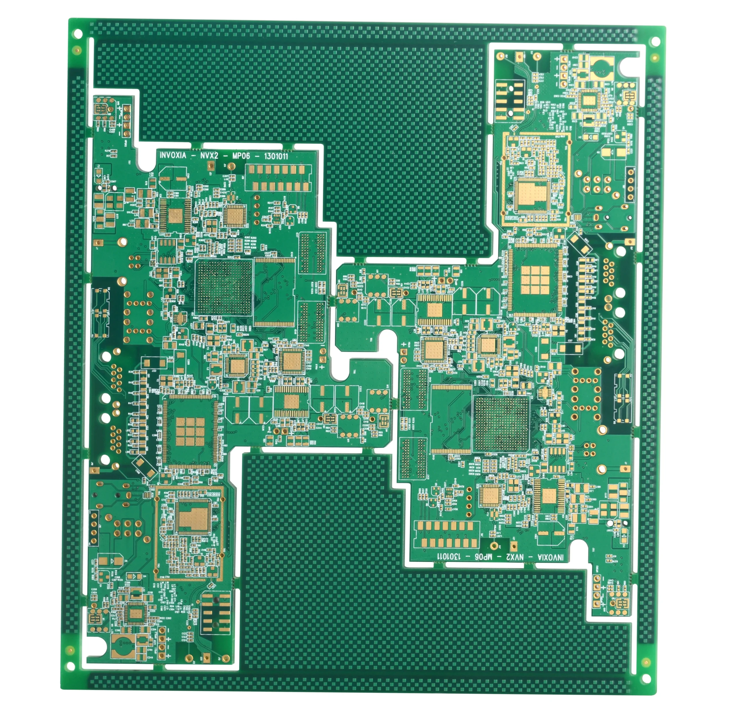
High-Frequency RF Design
Specialized materials and design rules for 5G, millimeter-wave, and ultra-wideband applications.
- ✓ Low-loss materials (Rogers, Isola, Panasonic)
- ✓ Via stitching & shielding design
- ✓ GHz-level signal integrity analysis
Thermal Management
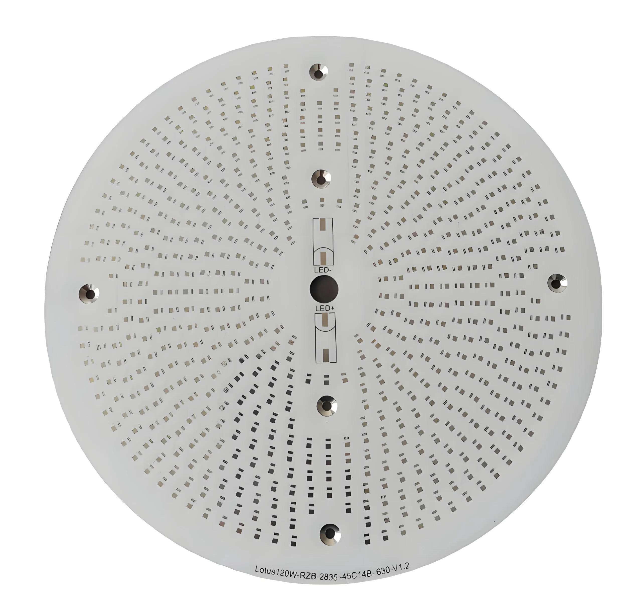
High-power applications with aluminum substrates, heavy copper, and thermal via design.
- ✓ Aluminum / Copper-based PCB with low thermal resistance
- ✓ Heavy copper up to 4oz (140µm)
- ✓ Thermal FEA simulation & optimization

High-Reliability & Mil-Grade
Aerospace, medical, and military-grade PCB manufacturing with enhanced process controls.
- ✓ IPC-A-600 Class 3 compliance
- ✓ Extended temperature range (-40°C to +125°C)
- ✓ Full traceability & lot testing
Flexible & Foldable PCB
Polyimide-based flexible circuits for consumer electronics, wearables, and innovative form factors.
- ✓ Flex down to 0.1mm thickness
- ✓ Foldable & multi-fold designs
- ✓ 100K+ fold cycle testing
Fast-Turn Prototyping
Rapid sampling and emergency production for time-critical projects without compromise on quality.
- ✓ Sample turnaround: 7-10 days standard, 3-5 days expedited
- ✓ 24/7 production scheduling
- ✓ Design feedback & DFM optimization
Not Sure What You Need?
Our engineering team can review your requirements and recommend the best PCB solution, material, and manufacturing approach.
Complete PCB Buying Guide
Step-by-step guide to help you source, evaluate, and purchase the right PCB from a reliable manufacturer
Define Your Requirements
- → Board Type: Single/Double/Multi-layer, HDI, Flex, Rigid-Flex?
- → Size & Shape: Dimensions, panelization, custom edge contours?
- → Technical Specs: Layer count, trace width, hole size, impedance?
- → Material: FR-4, Polyimide, Aluminum, special material?
- → Quantity: Sample, small batch, or mass production?
Request Quote & Samples
- → Prepare Files: Gerber files, BOM, assembly drawings, design notes
- → Get DFM Review: Free design-for-manufacturing analysis
- → Sample Turnaround: 3-5 days standard or 1-3 days expedited
- → Quotation Includes: Unit price, MOQ, lead time, shipping cost
- → NRE & Tooling: One-time charges for custom panelization
Evaluate & Approve
- → Sample Quality: Visual inspection, electrical test, thickness check
- → Compare Options: Check supplier certifications, lead times, flexibility
- → Negotiate Terms: Price, volume discounts, payment terms, warranty
- → Quality Assurance: Confirm testing protocols, inspection methods
- → Approval Order: Place sample approval order (usually 1-5 pieces)
Place Production Order
Once approved, move to full-scale manufacturing with confidence.
- ✓ Quantity Confirmation: Total number of pieces, packaging format
- ✓ Production Timeline: Lead time, batch split options, partial shipments
- ✓ QC Checkpoints: In-process inspections, final testing, documentation
- ✓ Payment Terms: Deposit, progress payment, final balance upon shipment
- ✓ Shipment Details: Destination port, incoterm (FOB, CIF, DDP), insurance
Receive & Verify
Final inspection before integration into your production.
- ✓ Package Inspection: Count, condition, labeling accuracy
- ✓ Incoming QC: Spot-check sample pieces, electrical continuity test
- ✓ Documentation: Packing list, invoice, quality certificates, test reports
- ✓ Storage & Handling: Proper PCB storage (temperature, humidity)
- ✓ Long-Term Partnership: Reorder support, design updates, volume discounts
Your PCB Buying Checklist
Before You Request a Quote
- Complete Gerber file set (with job notes)
- Design specifications & technical requirements
- Expected production volume & timeline
- Budget constraints or cost targets
- Quality & compliance requirements (RoHS, IPC, etc.)
When Evaluating a PCB Manufacturer
- ISO 9001 & IPC-A-600 certifications present
- Sample quality & delivery timeframe
- Equipment capabilities match your requirements
- Customer testimonials & reference accounts
- Transparent communication & responsive support
Frequently Asked Questions
Get answers to common questions about our PCB manufacturing, capabilities, and ordering process
What is your minimum order quantity (MOQ)? +
We have flexible MOQ policies:
- Samples: 1 piece or more (Depending on customer needs)
- Production Run: No hard minimum; Depending on customer needs
For prototyping and quick validation, we support sample orders with expedited service charges.
What are your lead times for sampling and production? +
Lead times vary based on complexity and volume:
| Type | Standard | Expedited |
| Sample (2-4 pieces) | 3-5 days | 1-3 days (+30%) |
| Small Batch (100-500) | 5-7 days | 3-5 days (+20%) |
| Production (1000+) | 10-15 Days | 7-10 Days (+15%) |
Times begin after Gerber file approval and payment. Complex designs (HDI, high-layer) may require +3-5 days.
Do you offer PCB Assembly (PCBA) services? +
Yes! We provide complete PCBA services including:
- ✓ PCB bare board manufacturing
- ✓ Component sourcing & procurement
- ✓ SMT (Surface Mount Technology) assembly
- ✓ Through-hole (DIP) component insertion
- ✓ Soldering, inspection, & testing
- ✓ Box build & final assembly
One-stop solution reduces complexity and ensures better integration. View PCBA Services →
What certifications and quality standards do you meet? +
We are certified and compliant with:
- ISO 9001:2015 - Quality Management System
- IPC-A-600 - PCB Acceptability Standard (Class 2 & 3)
- IPC-600 - Electrical Performance Specification
- RoHS 2.0 - Hazardous Substances Restriction
- UL (Underwriters Laboratory) - Safety certification (optional)
- ISO 14001 - Environmental Management
All certificates are available upon request, and we maintain full traceability for all materials and processes.
Can you handle custom or special PCB requirements? +
Absolutely! We specialize in custom solutions:
- ✓ Impedance control (±5-10%) for high-speed applications
- ✓ Heavy copper (up to 4oz) for high-current designs
- ✓ Flexible & foldable PCB designs
- ✓ Aluminum & copper-based PCB for thermal management
- ✓ HDI with micro vias and fine pitch components
- ✓ RF & high-frequency PCB (5G, mmWave)
- ✓ High-reliability aerospace & military-grade boards
Our engineering team will work with you to optimize design and manufacturability. Learn More →
How do you ensure quality control during manufacturing? +
Quality is built into every step of our process:
- Incoming Inspection: Raw material verification & batch testing
- In-Process QC: Automated Optical Inspection (AOI) at key stages
- Final Testing: 100% electrical continuity test + resistance measurement
- Environmental Testing: Temperature cycling, humidity, salt spray (optional)
- Traceability: Full lot traceability with batch documentation
- First-Pass Rate: Target 99.5%+ with <0.3% defect rate
What payment methods and terms do you accept? +
We offer flexible payment options:
- Payment Methods: Bank transfer (T/T), PayPal, Credit card, L/C (for large orders)
- Standard Terms: 50% deposit + 50% before shipment
- Flexible Terms: Full prepayment, net payment, or progress payments available
- Volume Discounts: Tiered pricing for recurring orders
- Long-term Partnership: Net 30/60 terms for qualified accounts
Contact our sales team to discuss payment terms tailored to your needs.
Do you provide technical support and design assistance? +
Yes! Our engineering team is here to help:
- ✓ Free DFM Review: Design-for-Manufacturing analysis of your files
- ✓ Technical Consultation: Material selection, stackup design, cost optimization
- ✓ Design Feedback: Recommendations for manufacturability & reliability
- ✓ 24/7 Support: Multi-language email & chat support
- ✓ Problem Solving: Fast response to production issues or urgent changes
Our engineers have 10+ years experience and can help you optimize everything from trace routing to layer stackup.
What is your warranty and what happens if there's a defect? +
We stand behind the quality of our products:
- Standard Warranty: 12 months from shipment date
- Defect Rate Target: <0.3% with full traceability
- Defect Resolution: Immediate replacement or refund for manufacturing defects
- Root Cause Analysis: Investigation and corrective action for repeated issues
- Documentation: Full test reports and inspection certificates provided
We take quality seriously and work closely with customers to prevent and resolve any issues quickly.
How do I place an order and what's the next step? +
Getting started is simple:
- Send Inquiry: Complete the quote form with your requirements
- Submit Files: Email or upload Gerber files, BOM, design specs
- Get DFM Review: Our engineer reviews files and offers recommendations (1-2 hours)
- Receive Quote: Detailed quotation with lead time and options
- Approve & Pay: Sign PO, submit deposit (50% standard)
- Production Starts: We confirm final specs and begin manufacturing
- Quality Check & Shipment: Final inspection and dispatch with tracking
Questions? Contact our sales team at any point in the process.
What file formats do you accept for PCB design? +
We accept the following file formats:
- Standard: Gerber files (RS-274X), Drill files (.TXT, .XLN)
- CAD Formats: Eagle (.BRD), KiCad (.KiCad_PCB), Altium (.PCB)
- Documentation: PDF assembly drawings, BOM in CSV/Excel, schematic PDF
- Additional: ODB++ (preferred for complex designs), STEP 3D models
Always include job notes (.txt) with layer definitions, special requirements, and assembly notes. Our CAM team will convert and optimize your files if needed.
Can you help reduce my PCB manufacturing costs? +
Absolutely! Our DFM engineers focus on cost optimization:
- ✓ Design Optimization: Recommend trace widths, vias, layer count to reduce cost
- ✓ Material Selection: Find cost-effective materials without sacrificing quality
- ✓ Panelization: Optimize panel design to reduce waste and labor
- ✓ Volume Discounts: Tiered pricing for increasing quantities
- ✓ Long-term Partnership: Recurring orders get special pricing
Didn't Find Your Answer?
Our team is ready to answer your specific questions and provide personalized guidance for your PCB project.
Send Your PCB / PCBA Requirements
Tell us what you need. For Gerber or ODB++ files, drill data, stack-up, BOM, CPL / pick-and-place files, assembly drawings or other attachments, email them directly to sales@ycelectronic.com after submitting this form.
 English
  Japanese
  French
  German
  Spanish
  Italian
  Portuguese
  Russian
  Dutch
Dutch  Turkish