 Skip to content
PCB & PCBA from One Factory Workflow Find Your Product Route First.
YC PCB helps purchasing and engineering teams reduce supplier risk by matching each PCB project to the right production route: fast standard PCB, engineering multilayer PCB, or high-difficulty PCB / PCBA review.
Factory-direct communication means DFM, fabrication, SMT, AOI, E-test, packing, and delivery records stay inside one workflow instead of being passed between middlemen.

Choose Your PCB Product Route First
Buyers need to know quickly whether we can make the product. Start here, then review lead time, DFM process, certifications, and RFQ details.
Fast Standard PCB
For standard FR4, aluminum PCB, copper base PCB, LED PCB, and simple double-sided boards.
Engineering Multilayer PCB
For multilayer PCB, HDI PCB, gold finger PCB, impedance control PCB, and industrial electronics.
High-Difficulty PCB & PCBA
For 20–40 layer PCB, rigid-flex, flexible PCB, heavy copper, high-speed boards, and turnkey PCBA.
Factory-Direct Means Capacity, Equipment, QC, and Delivery Traceability
Buyers should not rely only on the phrase “one factory workflow.” A real PCB factory should show production capacity, equipment ownership, inspection capability, and a visible production route from Gerber to shipment.
With dozens of production lines, smart PCB equipment, more than 100,000 m² monthly output capacity, and a dedicated team of 135+ experts, YC PCB supports prototype, small-batch, medium-batch, and large-batch production with factory-based quality control.
Production Equipment Ownership Matrix
Show factory-owned equipment by process stage. Add exact equipment quantities, model names, and capability ranges after internal audit.
| Process Stage | Equipment to Show | Capability to Prove | Buyer Risk Reduced | Image Slot |
|---|---|---|---|---|
| Front-end preparation | Cutting machine, grinding machine, cleaning line | Panel size control, surface preparation, laminate handling | Reduces material preparation and process-start variation | 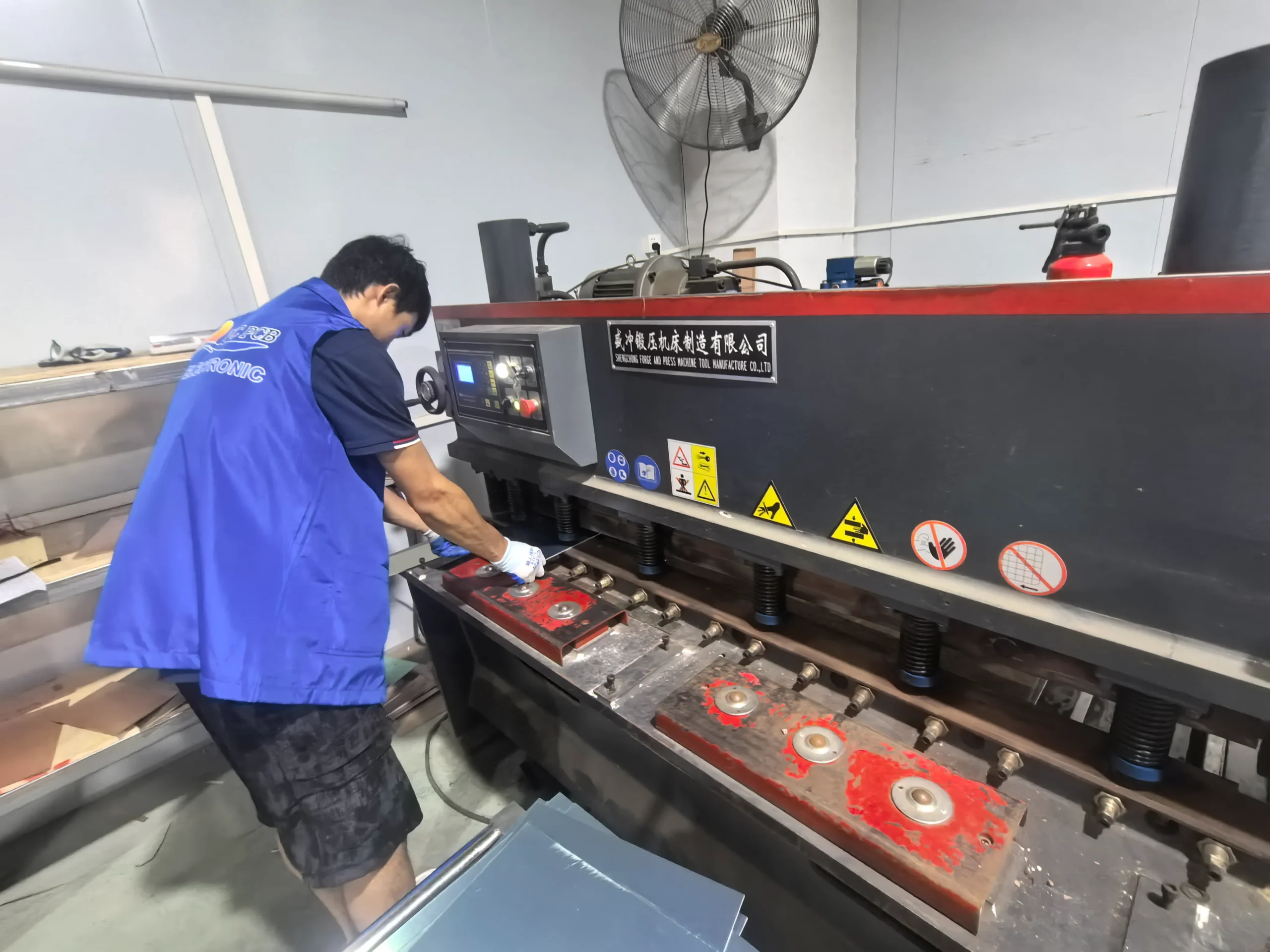 |
| Imaging and circuit formation | Exposure machine, etching line, solder mask, silkscreen | Trace definition, solder mask registration, marking clarity | Reduces open/short and solder bridge risk | 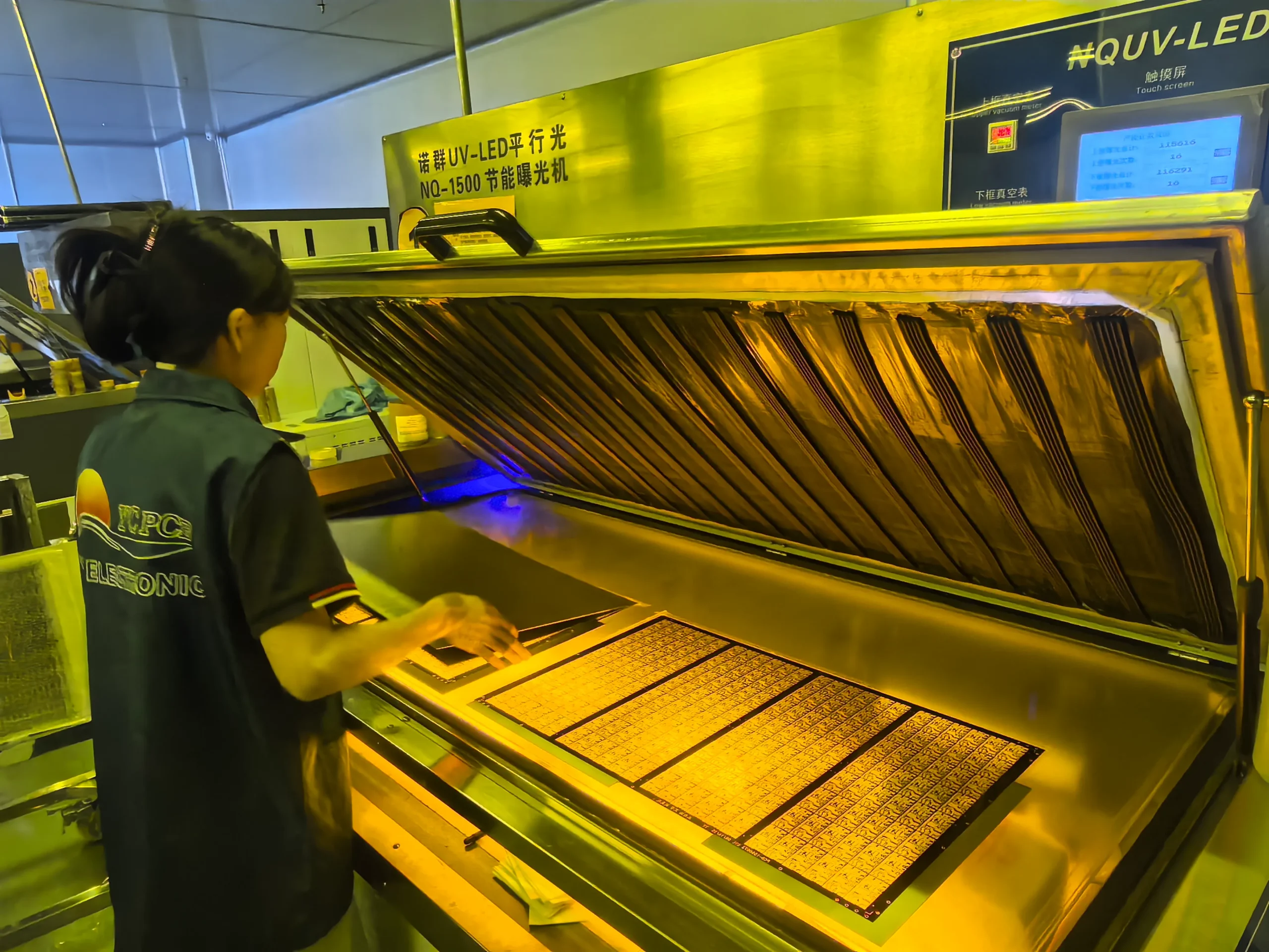 |
| Hole processing | Drilling machine, CNC machine, V-cut machine, routing | Via hole, mounting hole, outline, panelization, depaneling accuracy | Reduces assembly fit and mechanical tolerance risk | 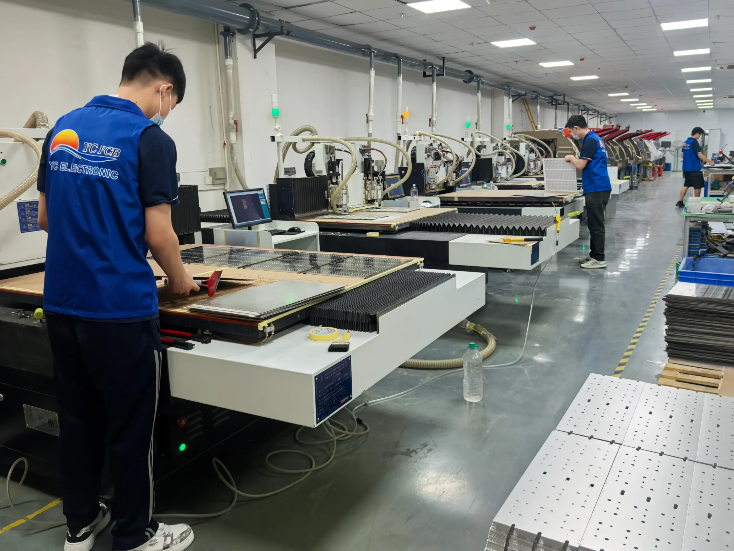 |
| Multilayer process | Lamination machine, punching, stack-up tooling | Layer bonding, stack-up consistency, warpage control | Reduces delamination and stack-up deviation risk | 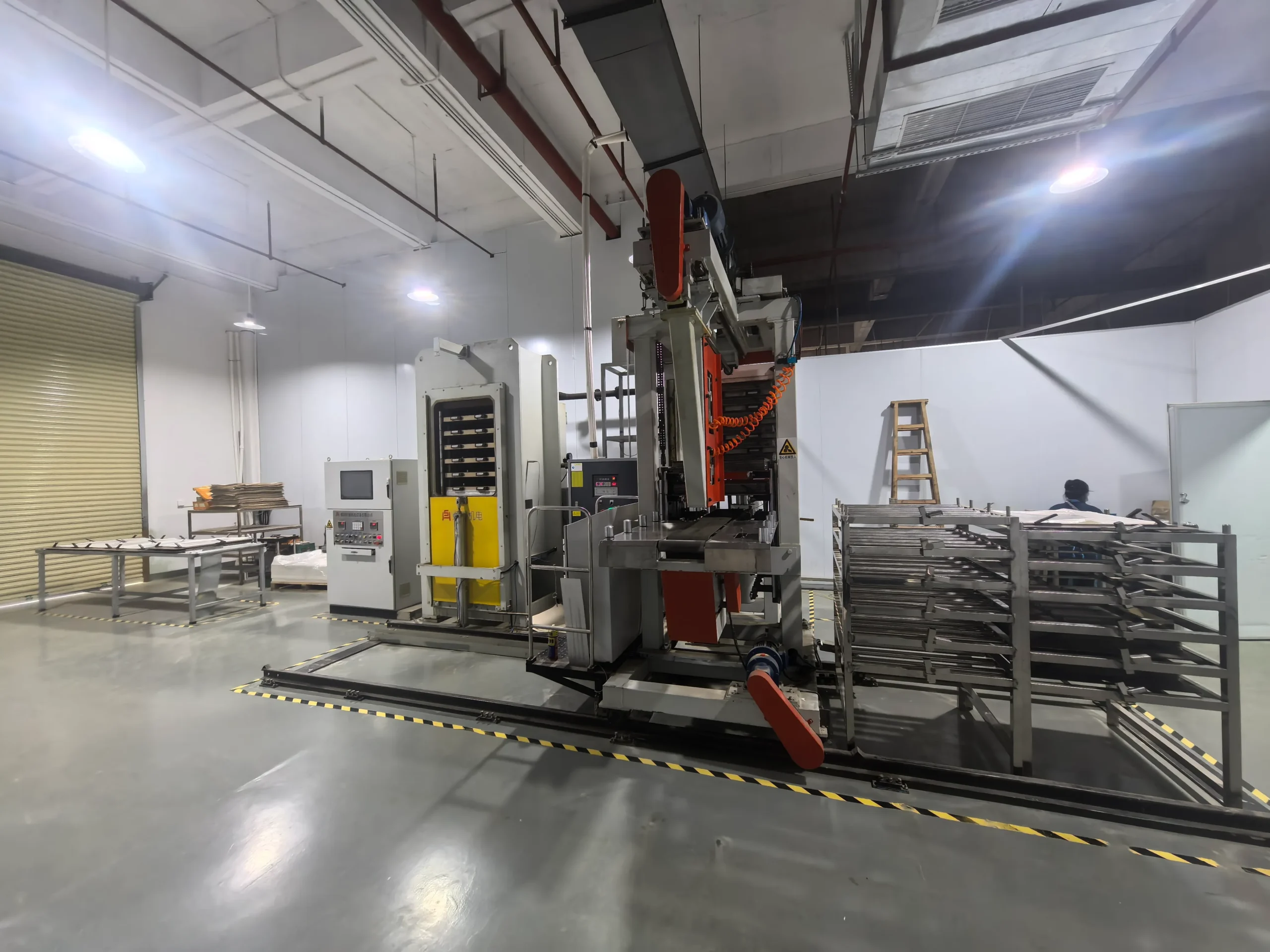 |
| Inspection and test | AOI, automatic electrical test, flying probe, X-ray if required | Open/short detection, visible defect screening, BGA and hidden joint check | Reduces shipment defect and hidden assembly risk | 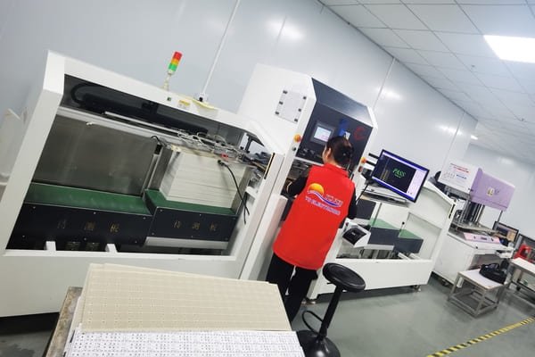 |
| PCBA production | SMT line, stencil printing, pick-and-place, reflow, DIP, FCT stations | Placement, soldering, assembly verification, functional test workflow | Reduces supplier handoff and BOM coordination risk | 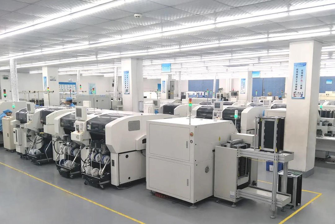 |

Cutting & Panel Preparation
Shows raw panel handling before drilling, imaging, and circuit formation.

Drilling / CNC Capability
Supports via, mounting hole, routing, and mechanical outline processing.

AOI Inspection
Checks circuit defects, visible abnormalities, opens, shorts, and process variation.

E-Test Before Shipment
Verifies connectivity and helps reduce open/short risk before packing.
More Than Equipment Photos: Each Machine Supports a Specific Manufacturing Checkpoint
YC PCB uses equipment evidence to prove real factory capability. The goal is not to show a random gallery, but to connect each machine with a process step, a capability point, and a buyer risk that it helps reduce.

Raw Materials
Supports laminate, copper, solder mask, and material batch confirmation before production.

Grinding Machine
Helps prepare board surfaces before imaging, solder mask, and follow-up process steps.

Exposure Machine
Transfers circuit patterns and supports trace definition before etching.

Etching Machine
Removes unwanted copper and forms circuit traces according to Gerber data.

Solder Mask Process
Protects copper traces and helps reduce solder bridge risk during assembly.

Automatic Shooting Machine
Supports automated processing and helps improve production repeatability.

Laminating Machine
Bonds multilayer PCB stackups under controlled production conditions.

Die Punching Machine
Supports board forming, punching, and repeatable production for suitable PCB outlines.

V Cutting Machine
Prepares panelized PCBs for efficient separation and assembly-line handling.
Drilling Machine
Creates vias, tooling holes, and mounting holes required by PCB drawings.
AOI
Checks visible circuit defects and helps prevent open/short issues before shipment.
Automatic Testing Machine
Verifies board connectivity and helps reduce shipment risk for finished PCBs.
PCB Fabrication Is Only One Part of the Factory Workflow
For buyers who need finished electronic products, YC PCB can coordinate PCB fabrication, component sourcing, SMT/THT assembly, IC programming, functional testing, and full product assembly in one project workflow.
PCB Assembly
Component sourcing, PCB fabrication, assembly, testing, and shipping with support for BGA, QFN, Micro-BGA, SMT, and THT packages.

Parts Management & Component Sourcing
Sourcing from trusted distributors such as Digi-Key and Mouser, with BOM review, shortage checking, and substitute approval support.

Functional Testing & Other Testing
ICT, FCT, environmental testing, and X-ray inspection can be selected according to project risk, package type, and customer acceptance plan.

IC Programming
Fast and secure IC programming before soldering, with NDA support for firmware and intellectual property protection.
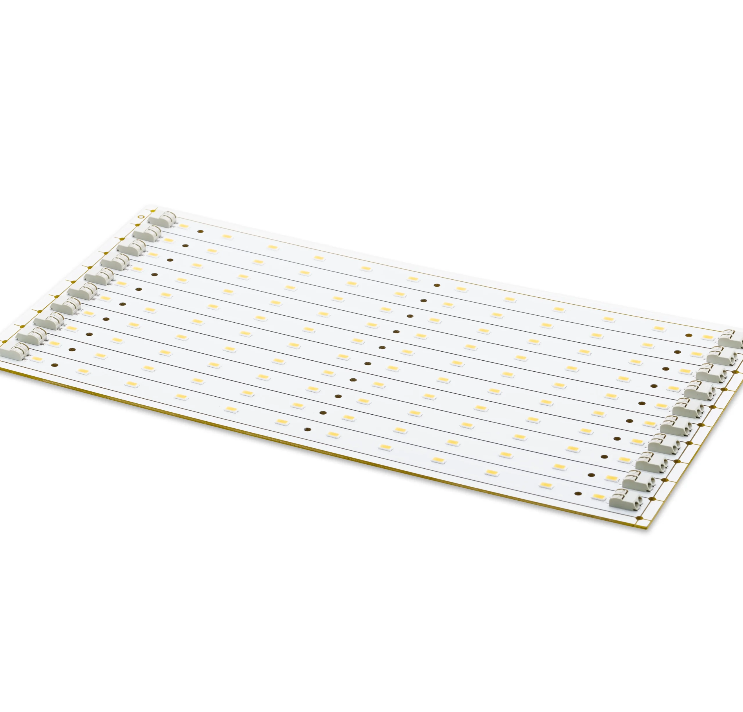
Full Product Assembly
Mechanical, electrical, and box-build assembly for OEM and ODM projects that need finished product delivery, not only bare boards.

Module Layout Design
Engineering support for module layout, production feasibility, assembly planning, and clearer product development communication.
From Gerber to Shipment: Process Steps Buyers Can Audit
This timeline replaces vague workflow language with checkpoints, responsible process stages, and inspection gates.
Gerber Received
File completeness, drill file, layer count, quantity, finish, and delivery target are checked first.
DFM & Production Route
Standard route, multilayer route, advanced engineering route, or PCBA BOM route is assigned.
Manufacturing
Cutting, drilling, imaging, etching, solder mask, lamination, surface finish, routing, and assembly when required.
QC, Packing, Shipment
AOI, electrical test, optional X-ray/FCT, final QC, ESD packing, carton label, and shipment record.
| Route | Typical Flow | Inspection Gate | Lead Time Logic |
|---|---|---|---|
| Standard PCB | File check → production → AOI / E-test → packing | AOI + electrical test | 1–5 days after approval |
| Multilayer PCB | DFM → stack-up → lamination → drilling → AOI / E-test | AOI + E-test + stack-up review | 5–12 days after DFM |
| PCBA | BOM check → PCB build → SMT / DIP → AOI / X-ray / FCT → packing | AOI + optional X-ray / FCT | 7–20 days by BOM |
All PCB & PCBA Products We Manufacture
Each product card now explains the buyer problem, the manufacturing solution, and the practical result. This helps engineers choose a route instead of reading a simple category list.
Fast Standard PCB Products
Good for fast prototype, LED lighting, consumer electronics, power modules, and cost-sensitive production.

Aluminum PCB
Buyer pain: LED and power boards overheat when FR4 cannot spread heat fast enough.
YC solution: aluminum substrate routes heat away from LED pads and power components while keeping cost lower than copper base.
Result: more stable thermal performance for lighting modules, drivers, and power boards.

Double-Sided Aluminum PCB
Buyer pain: some lighting or power modules need both thermal transfer and more routing space.
YC solution: double-sided aluminum structure supports thermal management with expanded circuit layout.
Result: better route density without abandoning the thermal substrate path.

Copper Base PCB
Buyer pain: high-power LED modules can exceed the thermal capacity of FR4 or standard aluminum PCB.
YC solution: copper base with confirmed dielectric layer, insulation, CNC path, and thermal route before production.
Result: safer production route for flashlight, projector, stage light, and high-power LED modules.

1–4 Layer FR4 PCB
Buyer pain: standard boards still fail when panelization, finish, or assembly notes are unclear.
YC solution: fast Gerber review confirms thickness, copper, finish, V-cut, routing, and test requirement.
Result: fast prototype and batch production for controllers, drivers, and industrial boards.
Multilayer, HDI & High-Speed PCB Products
Good for industrial control, telecom, automotive electronics, data communication, servers, and high-density applications.

6–12 Layer Multilayer PCB
Buyer pain: stack-up imbalance, drilling deviation, or copper distribution can cause delay or scrap.
YC solution: DFM checks stack-up, copper balance, via structure, and material route before lead-time commitment.
Result: more predictable production for industrial control and communication boards.

HDI PCB
Buyer pain: blind via, microvia, and high-density routing increase yield and inspection risk.
YC solution: engineering review aligns via structure, lamination sequence, drill capability, and test method.
Result: safer route for compact telecom, server, and high-density electronics projects.

Gold Finger PCB
Buyer pain: connector boards need plating consistency and edge reliability under repeated insertion.
YC solution: gold finger process review covers beveling, plating requirement, finish, and visual inspection.
Result: better fit for communication modules, memory cards, and edge connector applications.

Impedance Control PCB
Buyer pain: high-speed boards can fail when impedance targets are not matched to real stack-up materials.
YC solution: stack-up review checks dielectric, copper thickness, reference plane, and TDR reporting needs.
Result: stronger signal-integrity confidence for telecom and data applications.
Flexible, Rigid-Flex, PCBA & Automotive Products
Good for compact modules, dynamic bending, camera modules, automotive lighting, LED assembly, and finished electronic products.

Flexible PCB / FPC
Buyer pain: flexible circuits can fail at bend zones, connector tails, or stiffener alignment areas.
YC solution: review PI thickness, copper type, coverlay, stiffener, bend radius, and outline tolerance.
Result: clearer manufacturability path for cameras, wearables, and compact modules.

Rigid-Flex PCB
Buyer pain: transition-zone cracks and layer separation can make rigid-flex projects expensive to recover.
YC solution: engineering review checks bend direction, rigid-to-flex transition, stack-up, and reliability notes.
Result: lower first-order risk for medical, camera, wearable, and compact industrial designs.

Automotive PCB Assembly
Buyer pain: automotive boards need stable assembly, clear test scope, and component availability control.
YC solution: BOM review, SMT / DIP planning, AOI / X-ray options, and substitute approval before procurement.
Result: cleaner PCBA handoff for vehicle lighting, control modules, and industrial electronics.

LED PCBA / SMT Assembly
Buyer pain: LED assembly depends on thermal path, LED supply stability, soldering quality, and aging test scope.
YC solution: PCB fabrication, LED sourcing mode, SMT, inspection, and optional aging / function test are aligned together.
Result: fewer supplier gaps between bare board, LED procurement, assembly, and shipment.
One Factory Coordinates PCB, BOM, SMT, Testing, and Shipment
In a separated supply chain, buyers often manage the PCB factory, component supplier, assembly house, testing vendor, and logistics team by themselves. That creates hidden project-management cost.
YC PCB's PCBA route is designed to reduce this coordination load. If a component is short, the project team can adjust purchasing priority, suggest an approved substitute path, or align SMT scheduling before the delay becomes a shipment problem.
PCB supplier + component buyer + assembly shop + test vendor + logistics, often with unclear responsibility when a part is missing.
Gerber, BOM, SMT plan, AOI / X-ray / FCT scope, packing, and shipment are discussed in one RFQ route.
Lower communication load, faster exception handling, and clearer ownership when PCBA lead time changes.
Product Route Summary
Use this table to match product type, review mode, and RFQ path.
| Product Type | Typical Layer / Structure | Typical Lead Time | Main Risk Variable | Best RFQ Path |
|---|---|---|---|---|
| FR4 / Aluminum / LED PCB | 1–4 layers | 1–7 days | Material stock, panelization, finish | Quick quote |
| Multilayer / Impedance PCB | 6–20 layers | 5–12 days | Stack-up, copper balance, impedance | DFM + stack-up review |
| HDI / Heavy Copper / 20L+ | Advanced structure | 10–15 days | Microvia, thick copper, test reports | Engineering proposal |
| FPC / Rigid-Flex PCB | PI flex / rigid-flex stack-up | 8–15 days | Bend zone, coverlay, stiffener, transition zone | Engineer review |
| PCBA / LED PCBA / Automotive PCBA | PCB + BOM + SMT / DIP + Test | 7–20 days | BOM availability, substitute approval, FCT scope | BOM review + PCBA quote |
Fast Lead Time Needs Conditions and Evidence
The 1–3 day prototype route applies to standard files, standard materials, in-stock laminate, and no required customer redesign. For complex projects, lead time is confirmed after DFM and material review.
What 97.3% On-Time Delivery Means
Procurement teams need a clear definition, not just a strong number. Our on-time delivery record is presented as an internal tracking model that can be replaced with your latest real data when available.
On-time delivery means shipment completed within the confirmed lead time window, with a tolerance of ±1 working day after file approval, material confirmation, and payment confirmation. Customer redesign time and waiting time for missing files are not counted as factory production delay.
Tracked Order Breakdown
Replace these sample distribution numbers with your latest 12-month CRM / ERP export when available.
| Product Route | Sample Orders | On-Time Rate | Main Delay Reason |
|---|---|---|---|
| Standard PCB / 1–4L | 3-5 days | 99.2% | Panelization or finish change |
| Multilayer / 6–20L | 7-10 days | 96.8% | Stack-up or impedance confirmation |
| HDI / Rigid-Flex / PCBA | 7-10 days | 92.1% | BOM shortage or engineering approval |
Estimate Production Days After Choosing Product Type
This estimator is for RFQ screening only. Final lead time still requires Gerber review, material confirmation, production route approval, and payment confirmation.
Standard FR4 route with complete files and in-stock material. Final date depends on DFM approval and production slot.
DFM Review Explains Whether Your Design Is Safe to Produce
We review manufacturability, material route, stack-up feasibility, copper balance, assembly risk, and testing requirement before confirming the final lead time.
DFM Review Checklist
DFM Flow: Complete Files vs Missing Files
Gerber, drill, quantity, delivery target, and PCBA need are checked first.
File screening within working hours → DFM review in 4–24h for standard files → quote route confirmed.
Missing drill / stack-up / BOM / surface finish → missing-item list returned → waiting time is not counted as production delay.
HDI, rigid-flex, impedance, heavy copper, or PCBA BOM projects require extended engineering review before lead time is locked.
Why Some RFQs Get Delayed — and How to Avoid It
A complete first message can reduce quotation time sharply. These are the most common reasons a PCB or PCBA RFQ cannot be confirmed immediately.
Common RFQ Delay Reasons
Gerber without drill data can block hole-size, via, and plating review.
HASL, ENIG, OSP, and gold finger requirements change cost, lead time, and process route.
Multilayer and impedance boards need stack-up, dielectric, copper, and reference-plane information.
PCBA schedule depends on component availability. Substitutes require customer approval.
Fast RFQ Flow
Send Gerber + drill files
PDF drawings or ODB++ are helpful for multilayer, HDI, and impedance boards.
State one application sentence
Example: LED driver board, automotive lighting PCBA, industrial controller, camera FPC.
Add quantity, lead-time target, and destination country
This helps us check production slot and logistics route early.
Complete files + clear product type + quantity + delivery target.
Certifications & Quality Commitments for Procurement Review
Certification is not just decoration. It helps procurement teams verify quality systems, compliance route, material documents, and inspection standards before supplier approval.
How can I confirm the boards meet my specification?
- ✓ IPC-A-600 inspection reference can be used for bare PCB acceptance.
- ✓ Multilayer and HDI projects can add electrical test and stack-up related records.
- ✓ First article inspection notes can be aligned before batch shipment.
What happens if quality problems are found?
- ✓ RMA review can trace the issue to process stage, inspection record, or material batch.
- ✓ Failure analysis can include photos and root-cause summary when required.
- ✓ Corrective action follows the quality workflow instead of informal email replies.
What documents can procurement request?
- ✓ ISO certificate PDF and scope notes.
- ✓ UL / RoHS related document route by project.
- ✓ Inspection reports, E-test records, and packing photos when agreed.
| Certification / Standard | Procurement Protection | Scope to Verify |
|---|---|---|
| ISO 9001 Quality Management | Process control, document traceability, corrective action workflow | PCB manufacturing, PCBA assembly, testing, shipment process |
| UL Product Safety Support | Material and flammability verification for applicable PCB routes | Laminate, solder mask, board type, product route |
| RoHS / Material Compliance | Restriction of hazardous substances for export and industrial supply | Laminate, copper, solder mask, surface finish, assembly materials |
| IPC-A-600 / IPC-A-610 | Bare PCB and assembled board acceptability reference | Class 2 default / Class 3 by project approval |
Why Choosing YC PCB Is Easier to Defend Internally
A purchasing manager needs more than a low unit price. They need a supplier choice that can be explained to engineering, quality, and management if the project becomes urgent or complex.
Quality instability risk
Trace to production stage, inspection record, and process route instead of answering “we do not know.”
Delivery delay risk
Lead time is tied to product route, file completeness, material availability, and DFM status.
Technical support risk
Engineers review stack-up, copper, impedance, bend zone, or BOM risks before production starts.
Evidence Your Engineering and Quality Teams Can Accept
Buyers often need to justify a supplier choice internally. This section turns sales claims into operational evidence that engineering, quality, and management can evaluate.
Will the factory find design risks before production?
Use the DFM checklist and flow to show that file completeness, drill data, stack-up, copper balance, impedance, solder mask, and BOM risks are reviewed before production approval.
Can delivery and quality claims be verified?
Use the tracked-order breakdown, on-time definition, certificate slots, inspection record sample, and RMA response path as evidence for supplier approval.
What happens when a project changes urgently?
Factory-direct communication reduces the delay caused by middlemen. Engineering can re-check stack-up, material, panelization, BOM substitutions, and production slot in one workflow.
Factory-Direct vs Trading-Company Mode
The difference is not only price. It affects DFM speed, design-change cycles, quality traceability, PCBA coordination, and quotation transparency.
| Decision Factor | Factory-Direct YC PCB | Trading-Company Mode | Buyer Impact |
|---|---|---|---|
| Equipment ownership | Factory-owned process and inspection equipment such as drilling, AOI, electrical testing, CNC/routing, and SMT-related stations can be shown during supplier review | Testing and production proof may depend on outsourced factories, with slower access to records | Faster quality feedback and stronger audit confidence |
| Capacity flexibility | Internal production planning can adjust route, priority, and inspection load after engineering review | Schedule depends on another factory’s production queue and communication delay | Higher lead-time certainty for urgent orders |
| DFM feedback cycle | Engineer and production team can review directly | Files often need forwarding to the real factory | Less waiting before quotation |
| Design change response | Stack-up, copper, panelization, and test risks can be checked internally | Extra communication layer may add 1–3 days | Lower redesign delay |
| Quality issue traceability | Production, QC, packing, and delivery records can be traced inside one workflow | Root-cause investigation depends on another supplier | Faster corrective action |
| PCBA coordination | PCB, BOM, SMT, AOI, X-ray, and FCT can be aligned by one project team | Multiple parties may create communication gaps | Lower project-management risk |
Drilling Machine
Supports hole registration, via processing, routing accuracy, and mechanical hole production.
AOI Inspection
Checks trace defects, shorts, opens, and visible process issues before packing.
Automatic Testing Machine
Verifies board connectivity and helps reduce open/short shipment risk.
Send Files. Get Product Route + DFM Feedback.
For fast quotation, send your product type, Gerber files, quantity, delivery target, and PCBA requirement if needed.
RFQ Checklist
- • PCB type: FR4 / aluminum / copper base / HDI / FPC / rigid-flex / PCBA
- • Gerber + drill files
- • Layers, material, thickness, copper weight
- • Quantity, delivery target, destination country
- • BOM, pick-and-place, and test method if PCBA is needed
Engineering Contact
Add Gerber, BOM, drawings, photos, stack-up notes, or delivery targets to your message. A complete first message reduces quotation delay.

Ready to Start with a Factory-Direct PCB Supplier?
Send your Gerber, BOM, product type, quantity, and delivery target. YC PCB will review the right production route and reply with the next step.
 English
  Japanese
  French
  German
  Spanish
  Italian
  Portuguese
  Russian
  Dutch
Dutch  Turkish