 Skip to content
Multilayer PCB Manufacturing 4-40 Layer FR4, HDI, High-Speed, and Controlled Impedance.
For communication, industrial control, power electronics, and embedded systems.
DFM checks copper balance, via reliability, impedance, and lamination risk.
Recent 12-month delivery dataset: 97.3% on-time rate.
Certificate scans, AOI/e-test, TDR, and microsection samples.
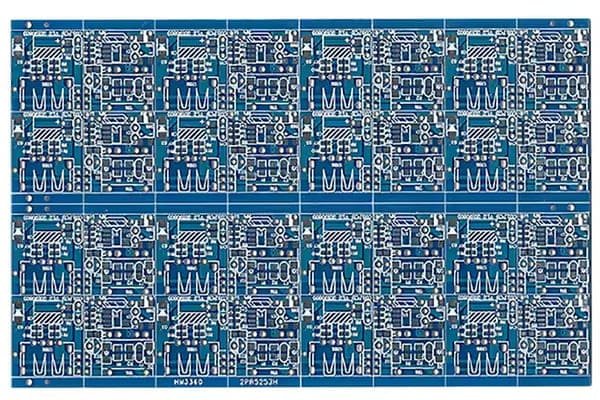

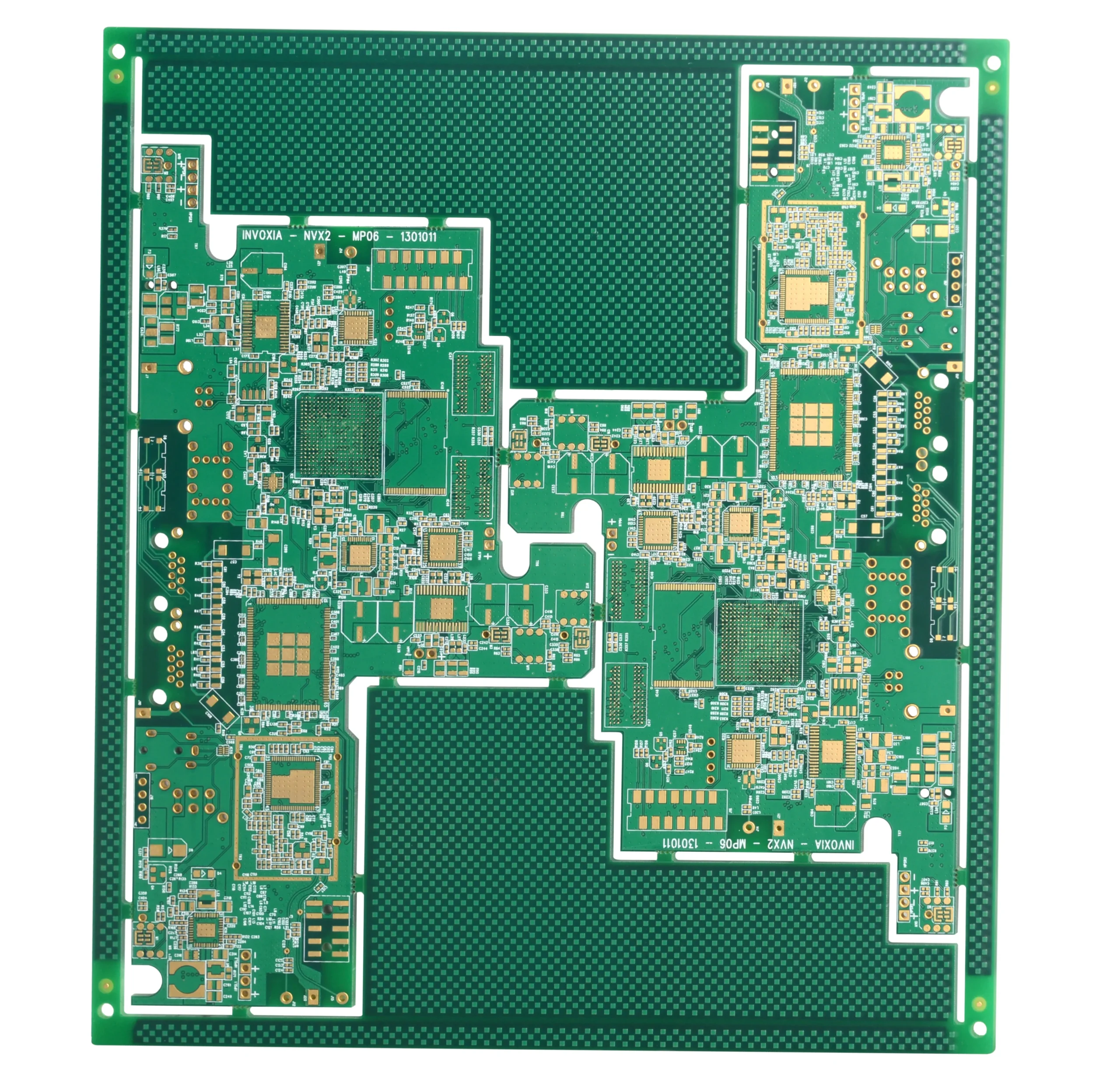
Choose the Multilayer PCB Type First
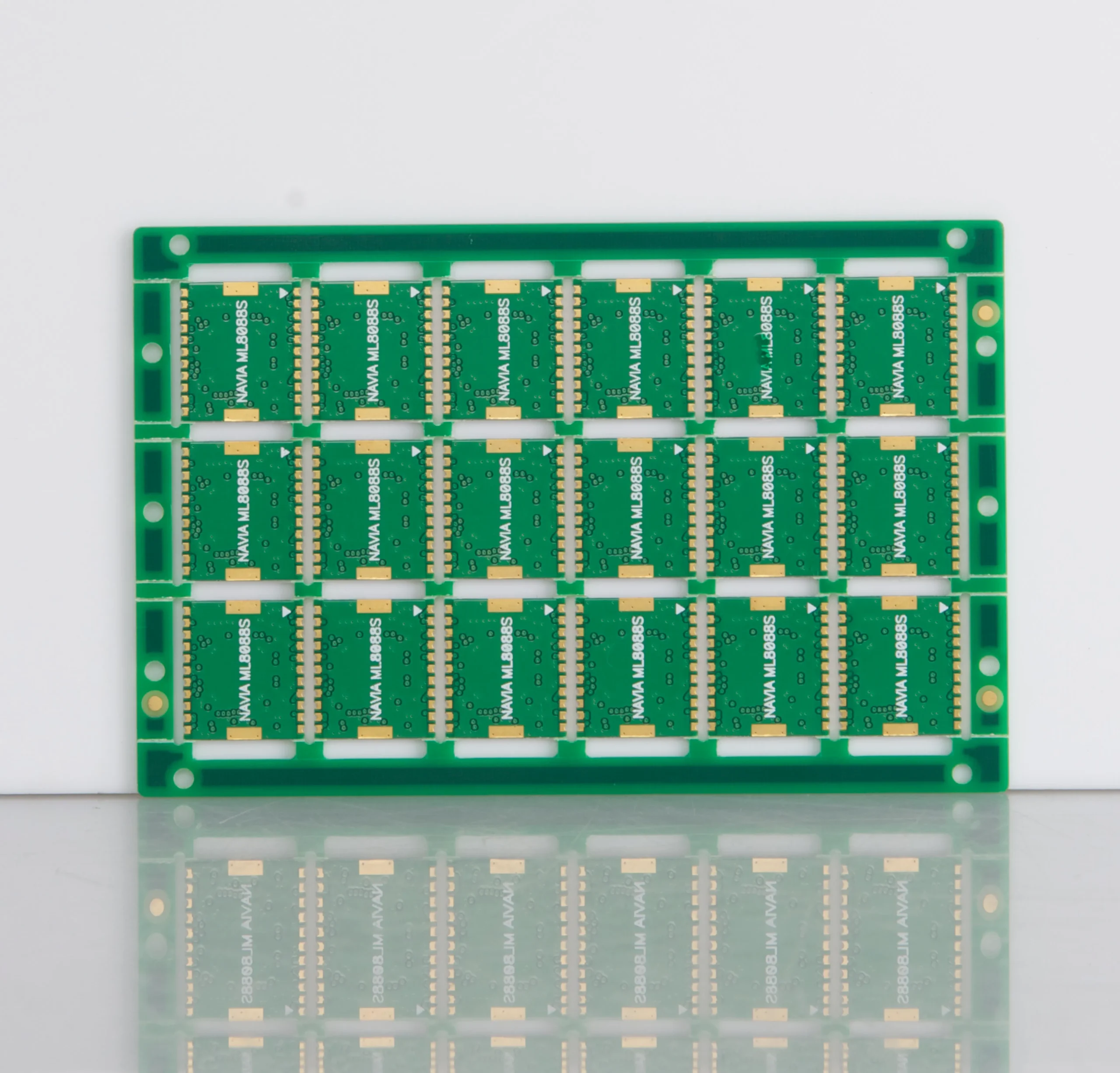
4-Layer FR4 PCB
For industrial control, power boards, control modules, and cost-sensitive multilayer projects.
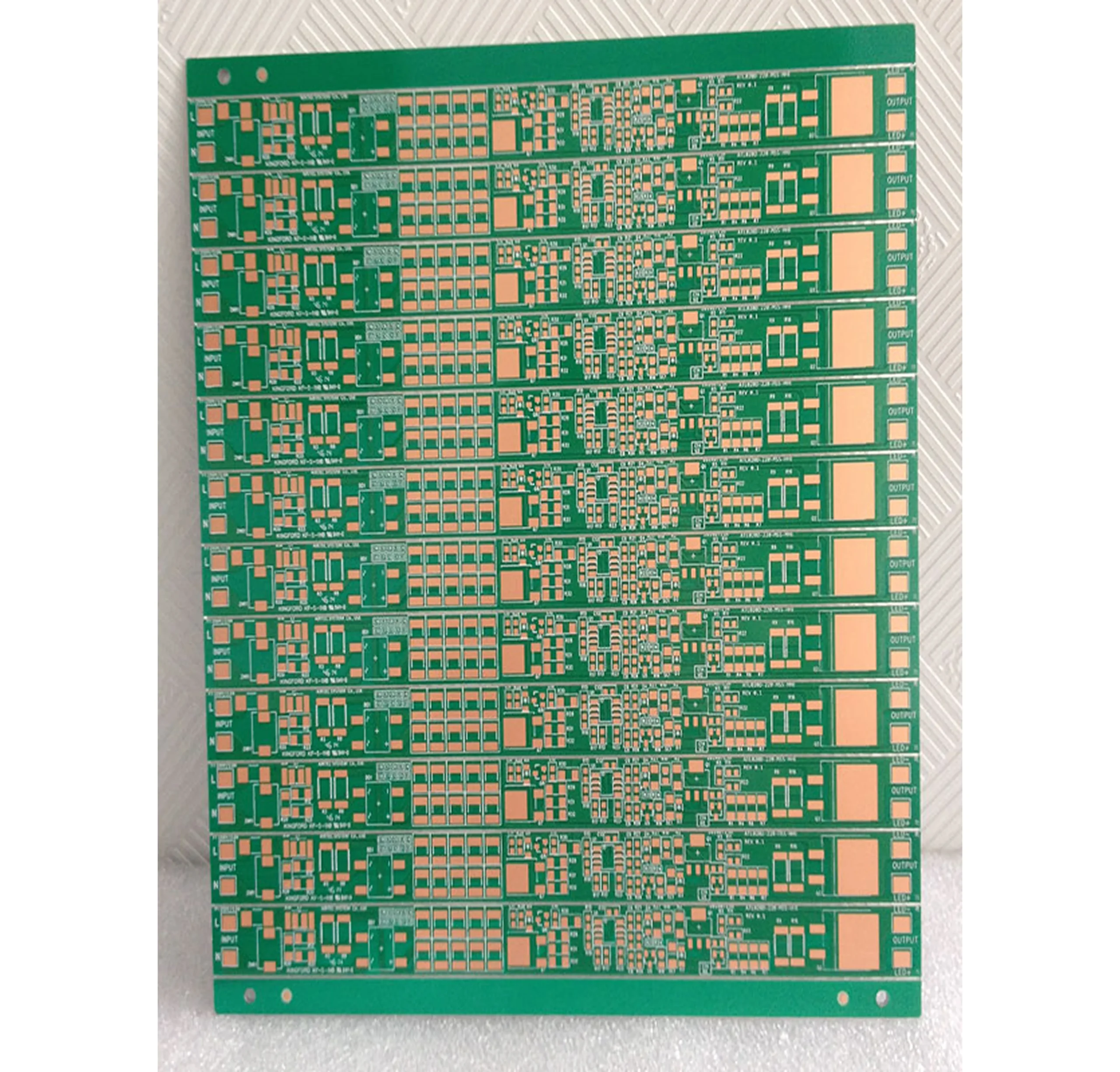
6-8 Layer PCB
For industrial control, communication boards, gateways, and embedded electronics.

High-Speed Impedance PCB
For communication modules, RF-related digital boards, backplanes, and high-speed control systems.
HDI / Blind-Buried Via PCB
For compact electronics requiring fine pitch, microvias, dense routing, and build-up structures.
Multilayer PCB Parameters
| Image | PCB Type | Layer | Material | Key Check | Surface Finish | Test Scope | Quote Condition | Quote |
|---|---|---|---|---|---|---|---|---|
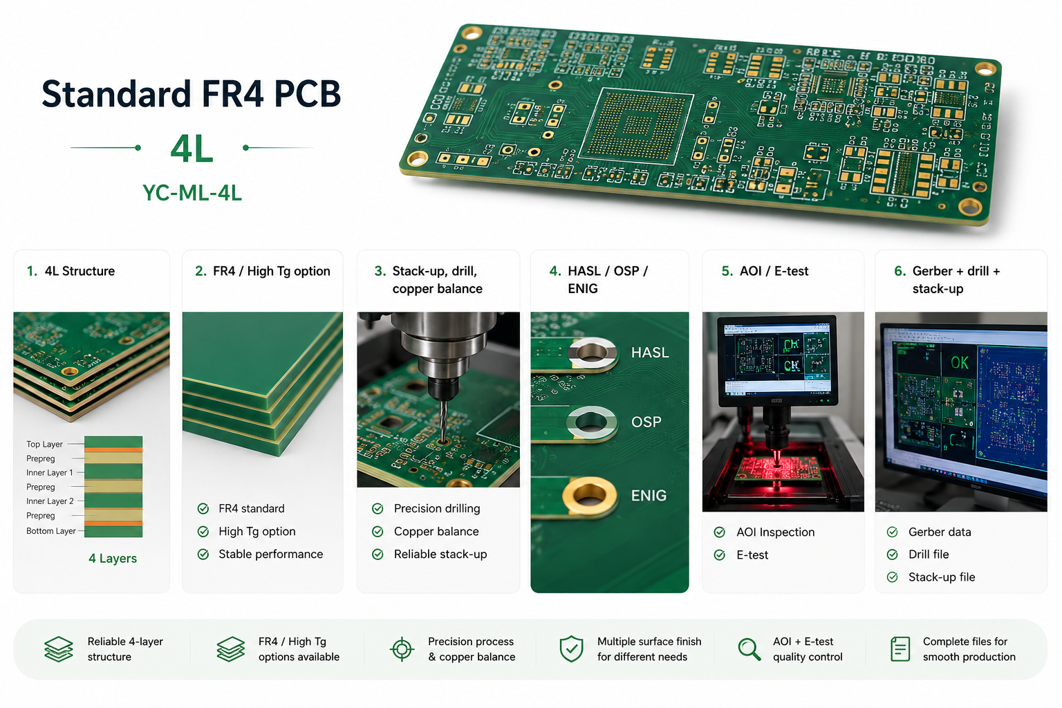 | Standard FR4 PCB YC-ML-4L | 4L | FR4 / High Tg option | Stack-up, drill, copper balance | HASL / OSP / ENIG | AOI / E-test | Gerber + drill + stack-up | |
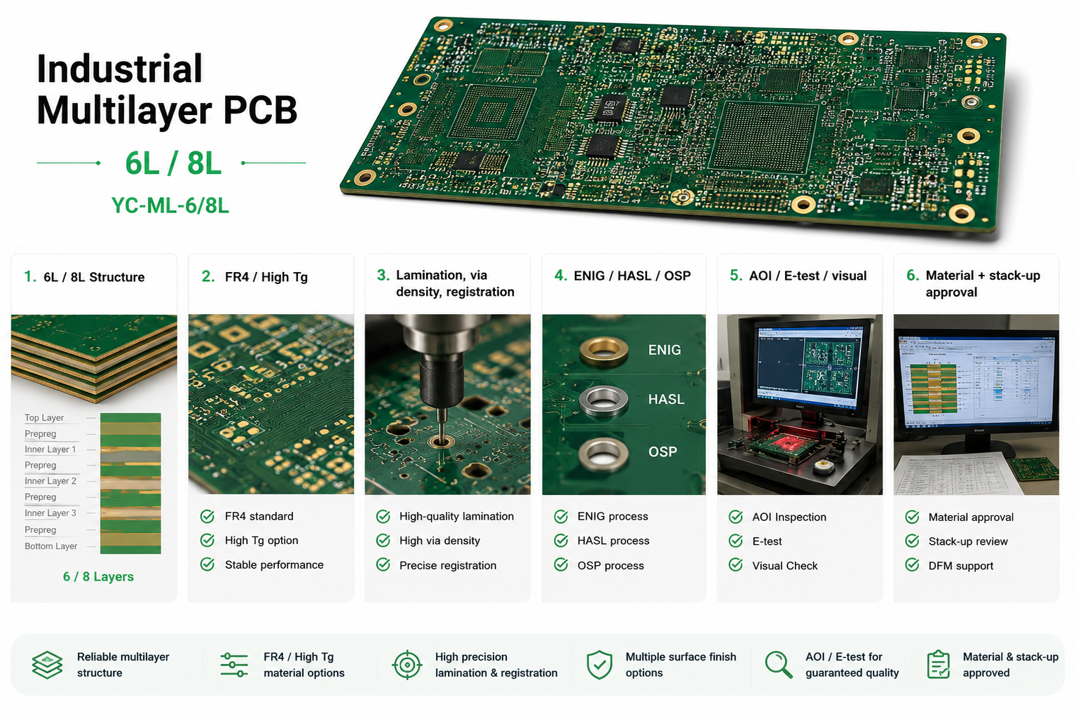 | Industrial Multilayer PCB YC-ML-6/8L | 6L / 8L | FR4 / High Tg | Lamination, via density, registration | ENIG / HASL / OSP | AOI / E-test / visual | Material + stack-up approval | |
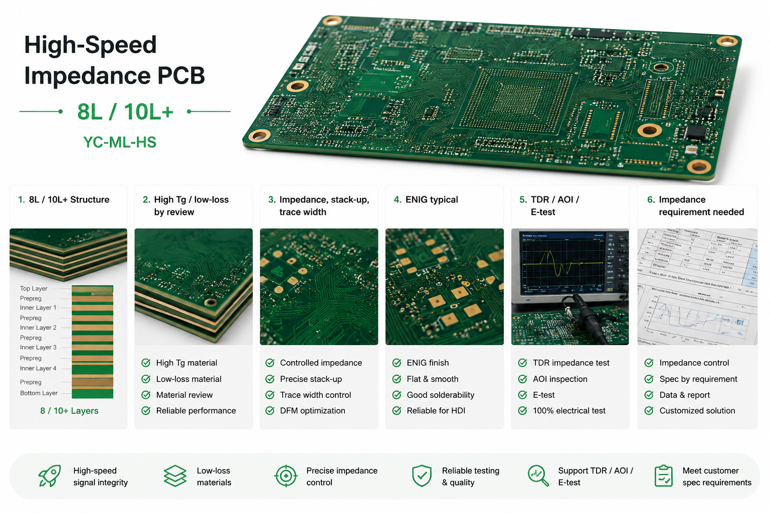 | High-Speed Impedance PCB YC-ML-HS | 8L / 10L+ | High Tg / low-loss by review | Impedance, stack-up, trace width | ENIG typical | TDR / AOI / E-test | Impedance requirement needed | |
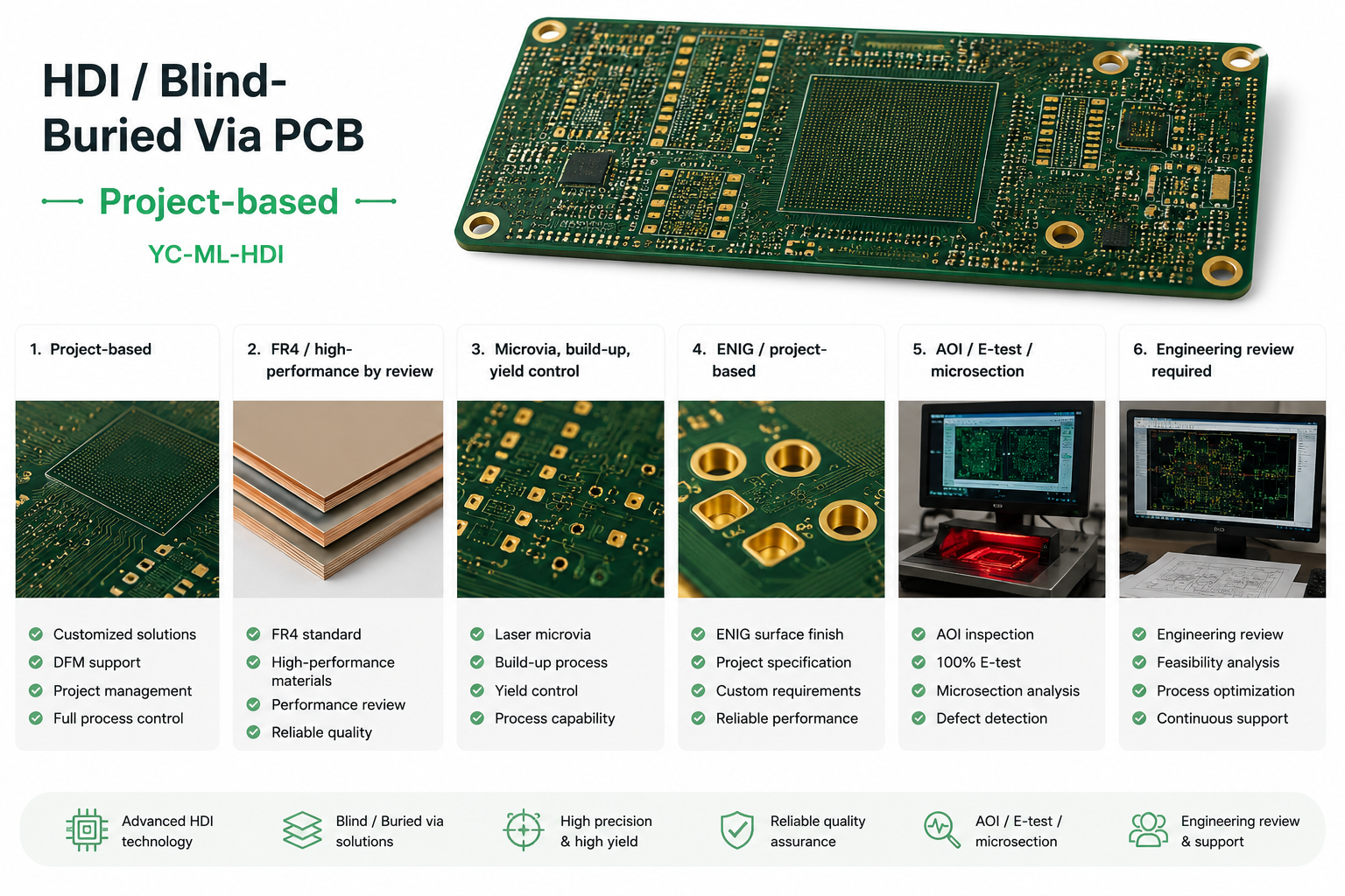 | HDI / Blind-Buried Via PCB YC-ML-HDI | Project-based | FR4 / high-performance by review | Microvia, build-up, yield control | ENIG / project-based | AOI / E-test / microsection | Engineering review required |
Final manufacturability depends on layer count, board size, dielectric thickness, copper weight, via type, impedance, finish, and test requirement.
Multilayer PCB Cost Is Matched by Risk Level, Not Public Unit Price
Public price references are misleading for multilayer PCB because copper weight, surface finish, impedance, trace/space, copper balance, via structure, lamination cycle, yield risk, and test scope can change cost sharply. The correct workflow is to route the buyer to the right quotation path.
Why We Removed the Public Cost Calculator
A simple layer × area × quantity formula can deviate by ±40% for impedance, HDI, heavy copper, high Tg, dense drill, or low-yield structures. It creates false precision for procurement teams. This page now uses quotation-path matching instead.
Cost Matching Path
Low process risk. Suitable for prototype and small-batch orders under standard FR4, normal copper, and non-impedance structures.
Medium process risk. Needs stack-up, copper balance, via density, surface finish, and material confirmation before quote accuracy is useful.
High process risk. Requires engineering proposal, test plan, possible sample approval, and project-specific quotation.
Multilayer PCB Quality
ISO, UL, and RoHS are necessary, but they do not directly prove stack-up stability, impedance accuracy, via plating reliability, or lamination yield.
4-layer PCB
Impedance-controlled PCBs
HDI PCB
ISO 9001 Protection
Protects process documentation, traceability, corrective action, and quality record control.
UL Documentation Protection
Supports laminate safety file, flammability-related documentation, and buyer audit requirement.
RoHS Protection
Protects material compliance for lead, cadmium, mercury, and restricted substances.
Delivery Commitment and Verification Method
| PCB Route | Typical Lead Time Logic | Main Risk | Verification Record | Packing Method |
|---|---|---|---|---|
| 4-layer FR4 prototype | After Gerber + stack-up approval | File mismatch / drill tolerance | DFM reply + e-test record | Vacuum + ESD + carton |
| 6-8 layer batch | After material + lamination review | Lamination yield / copper balance | AOI + e-test + packing photo | Vacuum + label control |
| 10+ layer high-speed PCB | After stack-up + impedance confirmation | Impedance tolerance / registration | TDR report + microsection by request | Project-specific packing SOP |
| HDI / blind-buried via PCB | Engineering-confirmed only | Laser via / build-up / yield control | Engineering report + test data | ESD + moisture protection |
Order Delivery

Sample Order A

Sample Order B

12-Month Delivery Dataset
Talk to Engineering Before Full Stack-up Release
Multilayer PCB projects often require a person to confirm stack-up, impedance, via structure, material, and production risk before a formal RFQ.
Engineering / Sales Contact
Reduce the Risk of First Cooperation
Multilayer PCB sourcing risk is not only price. Impedance failure, delamination, registration issues, and late delivery can stop the downstream schedule. Add the risk terms below into the quotation or PI before production.
Commercial Protection Terms
If the confirmed production shipment date is delayed by more than 3 working days due to YC PCB production causes, a 5% first-order credit can be written into the quotation.
For confirmed manufacturing defects, replacement / rework / credit handling follows the approved inspection record and signed quality agreement.
For high-risk 10L+ / HDI / impedance PCB, sample approval can be required before batch production release.
Final commercial protection terms should be confirmed in the quotation, PI, or supply agreement. Replace these terms with your approved company policy before publishing.
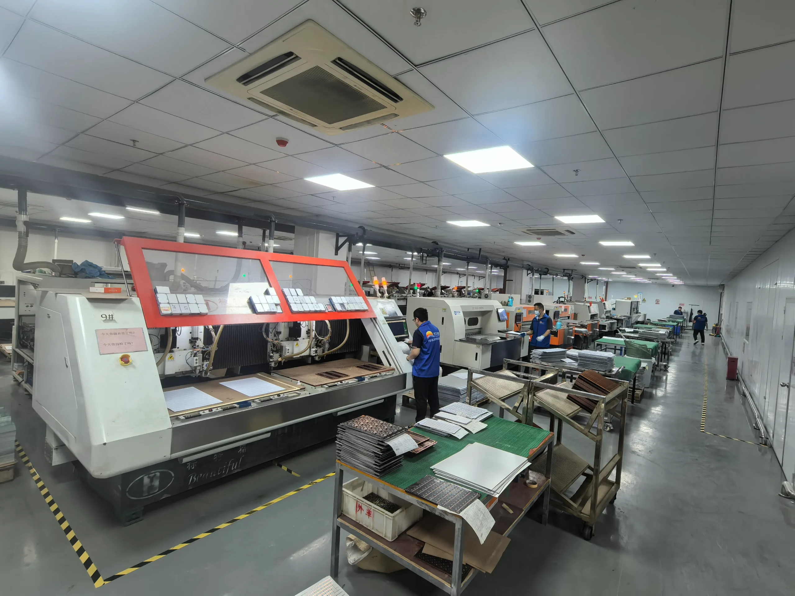
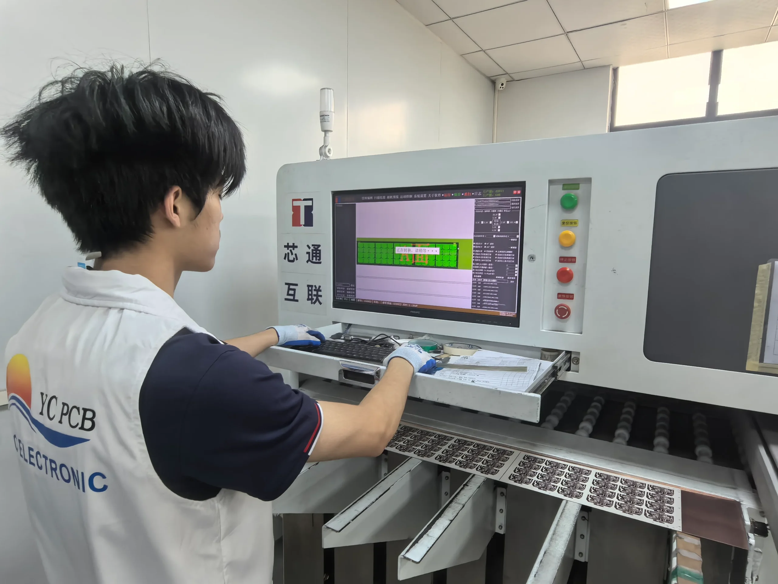
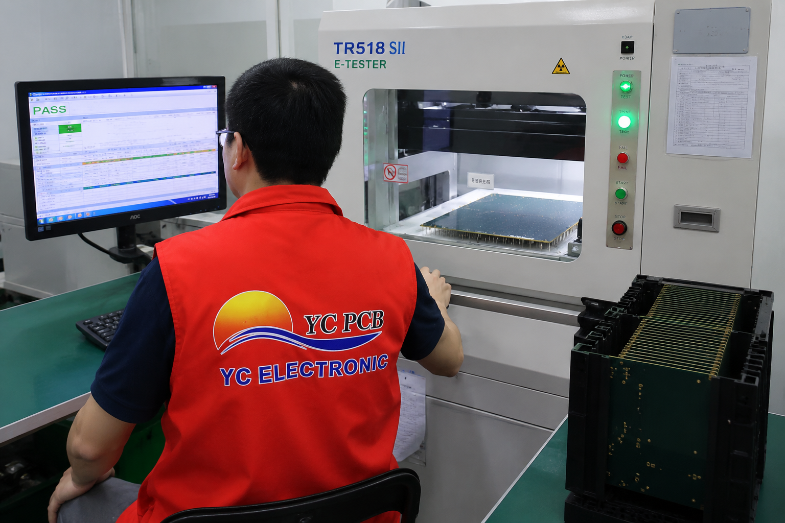
Real Photos for Multilayer PCB Technical Trust
DFM Review SLA Depends on File Completeness
A single absolute 24h DFM promise is risky for multilayer PCB. The SLA starts only after the input package is complete enough for engineering judgment. The rules below reduce expectation mismatch for international buyers.
| Workflow Step | Timing | Output | Buyer Decision |
|---|---|---|---|
| File completeness check | 60 min after receipt during working hours | Green / Yellow / Red status | Supply missing input if required |
| Engineering DFM | 24h for Green status files | Stack-up, impedance, copper balance, via risk review | Approve, reject, or revise |
| Improvement advice | Included in DFM result | Non-mandatory manufacturability advice | If accepted, add 1 working day for revised-file confirmation |
| Sample approval failure | New review cycle | Failure reason + corrective action proposal | Re-approve files and reset production lead time |
| Production release | After buyer approval | Signed DFM result + confirmed quote + lead time | Production starts |
Request a Multilayer PCB Quote
Send layer count, board size, quantity, material, stack-up, impedance requirement, surface finish, and Gerber/drill files.
Email: sales@ycelectronic.com | Website: ycpcbs.com
Send Your Multilayer PCB Requirements
Tell us what you need. For Gerber files, drill data, stack-up drawings, impedance tables, mechanical drawings, BOM or other attachments, email them directly to sales@ycelectronic.com after submitting this form.
 English
  Japanese
  French
  German
  Spanish
  Italian
  Portuguese
  Russian
  Dutch
Dutch  Turkish