11月 8, 2026
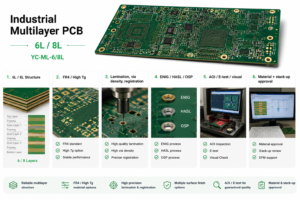
Multilayer PCB design from the fabricator's side: how layer count, stack-up symmetry, via structure and copper weight become production constraints.
続きを読む →
11月 8, 2026
Controlled impedance is a stack-up outcome, not a number on a drawing. Confirm planes, dielectric thickness, geometry and coupons before…
続きを読む →
11月 8, 2026
Differential pair design from the fabrication side: impedance targets, coupling, length-matching tolerances, reference planes and the data needed.
続きを読む →
11月 8, 2026
An HDI PCB design review checklist for engineers and buyers: microvia rules, stack-up sequencing, BGA escape routing, impedance and the…
続きを読む →
11月 8, 2026
What to send for a controlled impedance PCB quote: stack-up, impedance table, reference planes, material and coupon requirements, and why…
続きを読む →
11月 8, 2026
Export manufacturing files from KiCad correctly: which layers to plot, Gerber and Excellon drill settings, unit and origin traps, and…
続きを読む →
2025年1月8日
PCB設計の効率と品質を向上させるにはどうすればよいでしょうか?プリント基板(PCB)の設計は複雑な作業です…
続きを読む →




 Japanese
 English
 French
 German
 Spanish
 Italian
 Portuguese
 Russian
 Dutch
 Turkish