 Skip to content
PCB Factory & Manufacturing Capabilities
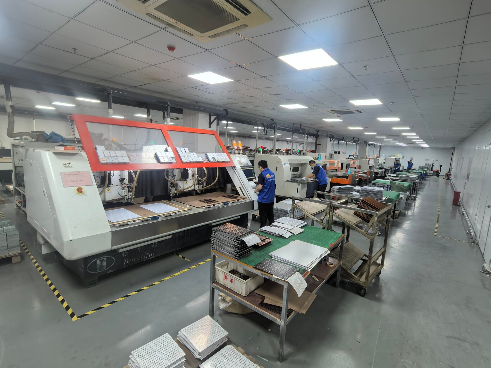
Source your PCB and PCBA projects from a manufacturing team that controls each critical stage—from incoming material and circuit imaging to drilling, lamination, solder mask, routing, AOI, electrical testing and assembly verification. Review our production equipment, quality checkpoints and order workflow before sending your project files.
Years of PCB and PCBA manufacturing experience
Engineering, production and quality support team members
Monthly PCB manufacturing capacity for prototype and batch projects
High-layer-count PCB projects reviewed by stack-up and design files
PCB Manufacturing Capabilities for Reliable Project Delivery
Your project is supported by a complete manufacturing route covering material preparation, image transfer, copper processing, multilayer lamination, drilling, routing, inspection and PCBA verification. Each stage is matched to your Gerber files, stack-up, quantity and quality requirements.
Material Control
Laminate type, board thickness, copper weight and material batch information are checked before production begins.
Controlled Production Route
Your boards move through a defined route covering cutting, imaging, etching, lamination, drilling, routing and surface processing.
Quality Gates
AOI, electrical testing and PCBA verification are arranged at key quality checkpoints before shipment.
Flexible Order Support
Prototype, pilot-run and batch orders are reviewed according to your drawings, quantity, technical requirements and delivery plan.
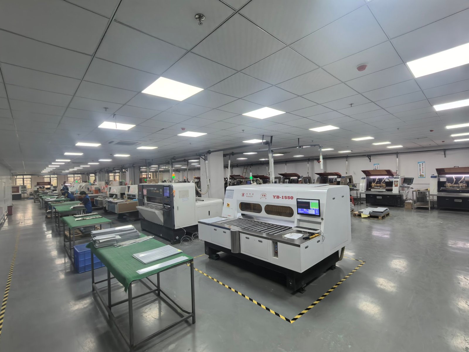
Organized PCB and PCBA Production Areas
Organized production areas, visible manufacturing equipment and defined inspection routes help us support consistent PCB fabrication and assembly from prototype verification to repeat orders.
PCB Production Line by Manufacturing Stage
Review the equipment used across material preparation, circuit formation, multilayer processing, mechanical finishing, testing and assembly. These processes help us match your design files with the correct manufacturing route.
Material Preparation
Controlled material preparation helps maintain correct panel dimensions, clean surfaces and stable material conditions before circuit processing begins.

Raw Material Area
Laminate and copper-clad materials are prepared by project specification, including material type, thickness, copper requirement and production batch.
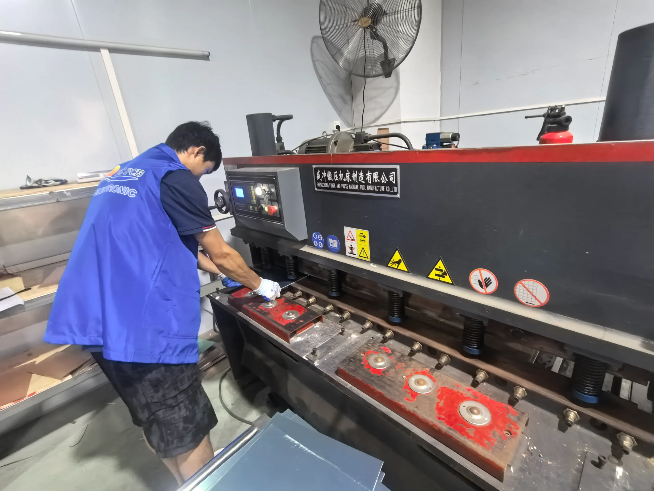
Cutting Machine
Accurate panel cutting prepares the required production size and supports alignment through imaging, drilling and final routing.
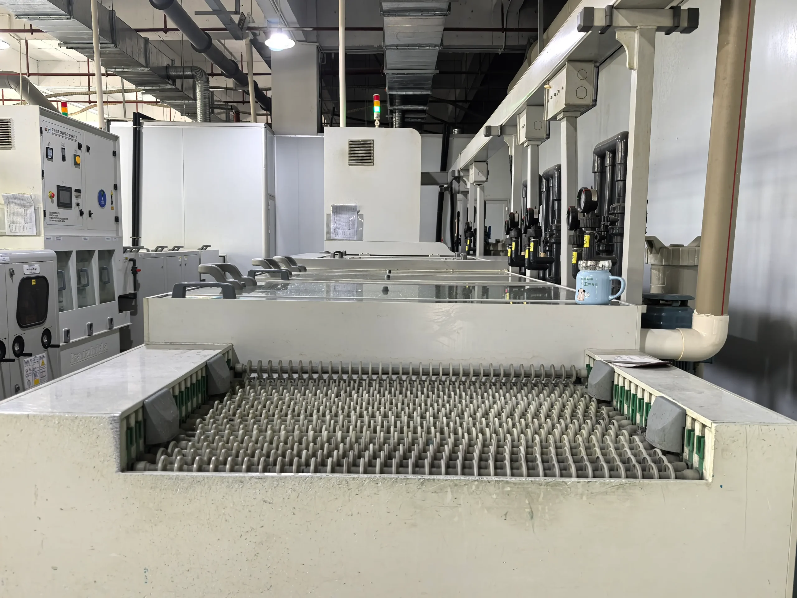
Grinding Machine
Panel grinding and surface preparation remove contamination and improve consistency for imaging, etching and later copper processing.
Circuit Pattern Formation
Exposure, etching and AOI work together to form the required copper pattern and identify circuit defects before additional processing adds cost and lead time.
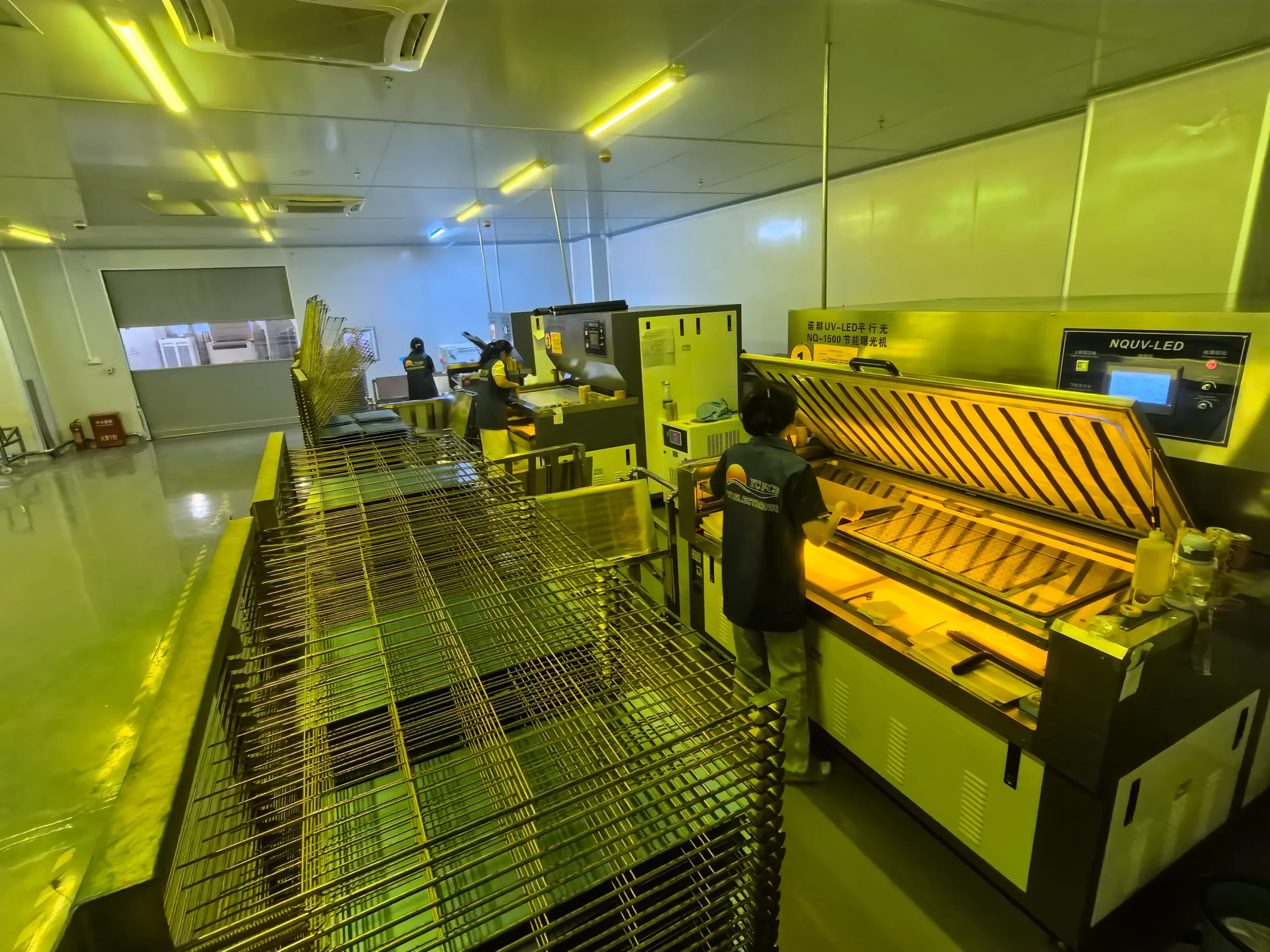
Exposure Machine
Controlled exposure transfers your circuit pattern to the panel and supports trace definition, spacing accuracy and layer registration.
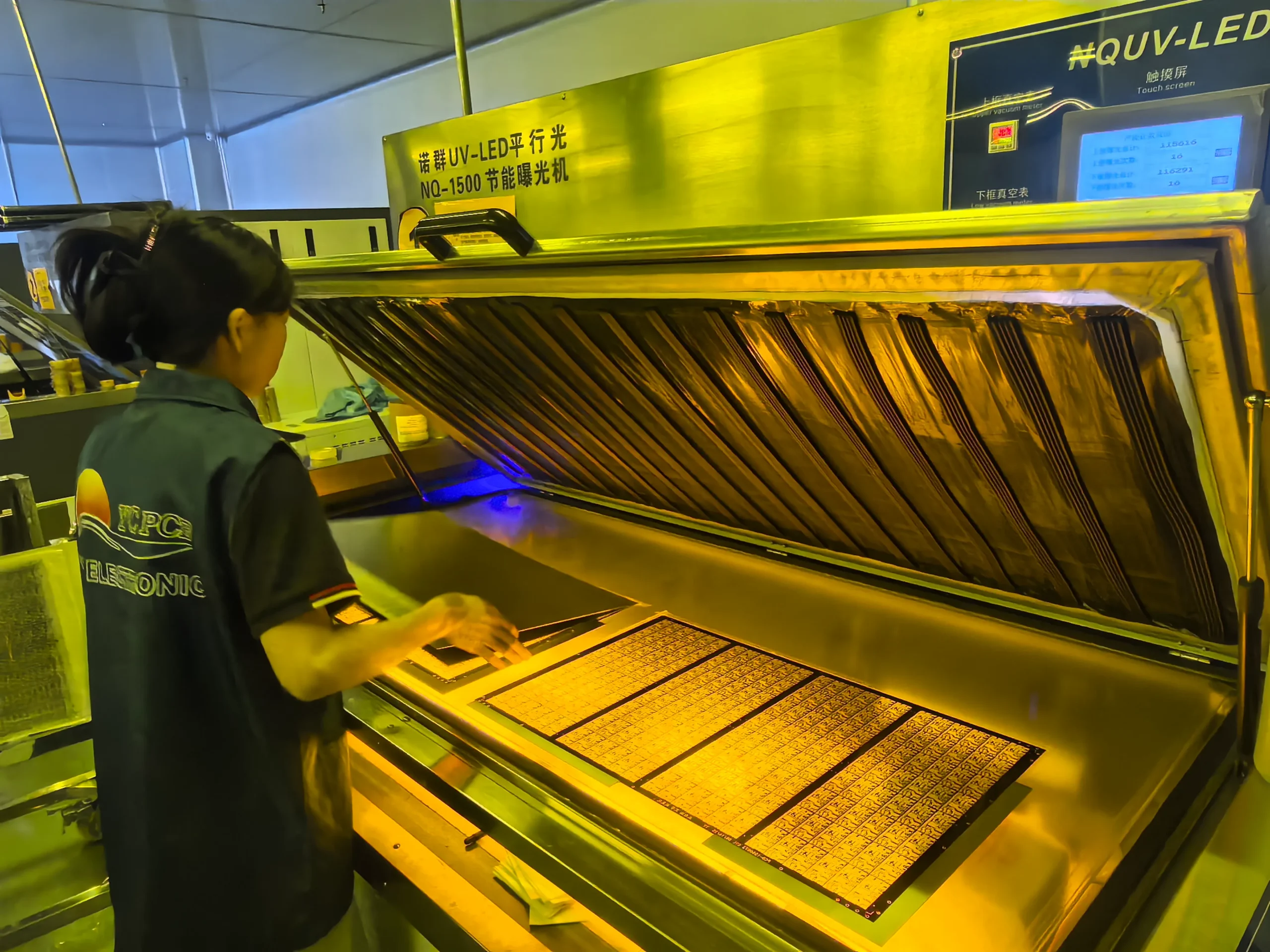
Exposure Process Area
Repeatable exposure control supports different board dimensions, circuit densities and production quantities.
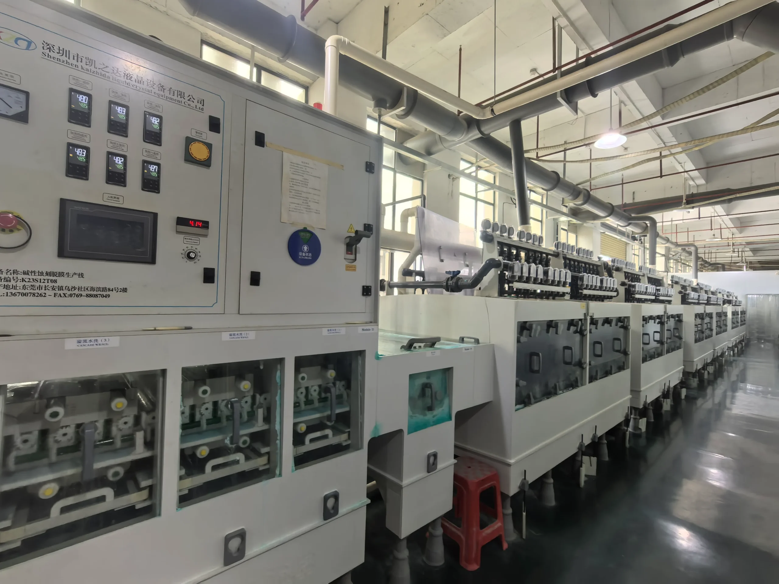
Etching Machine
Etching removes unwanted copper to create the required traces, pads and circuit features from your production files.
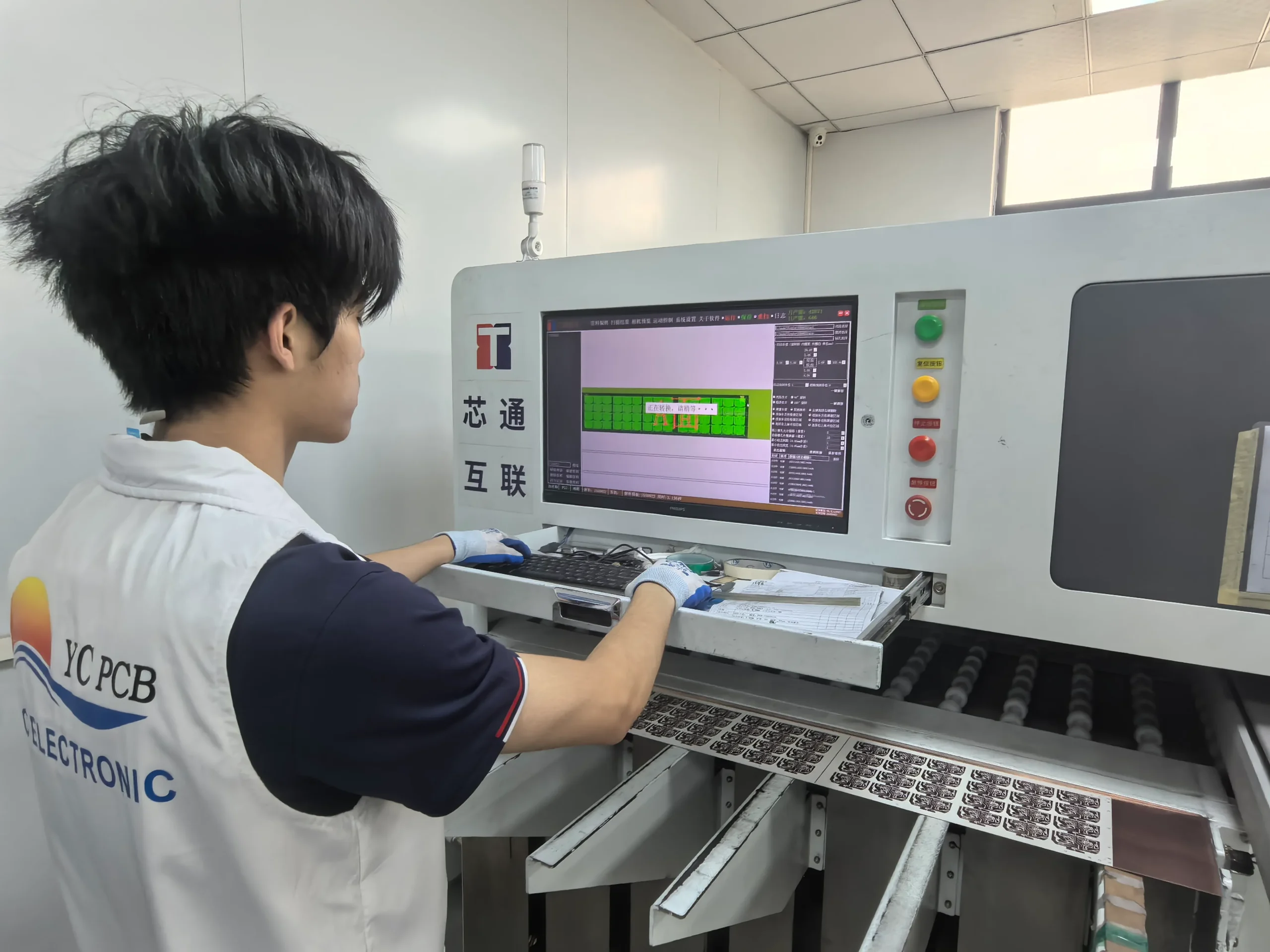
AOI Inspection
AOI checks for opens, shorts, missing copper and pattern deviations before the board enters later manufacturing stages.
Multilayer and Mechanical Processing
Controlled lamination, drilling and profile processing support layer registration, via reliability and accurate mechanical fit in your final assembly.
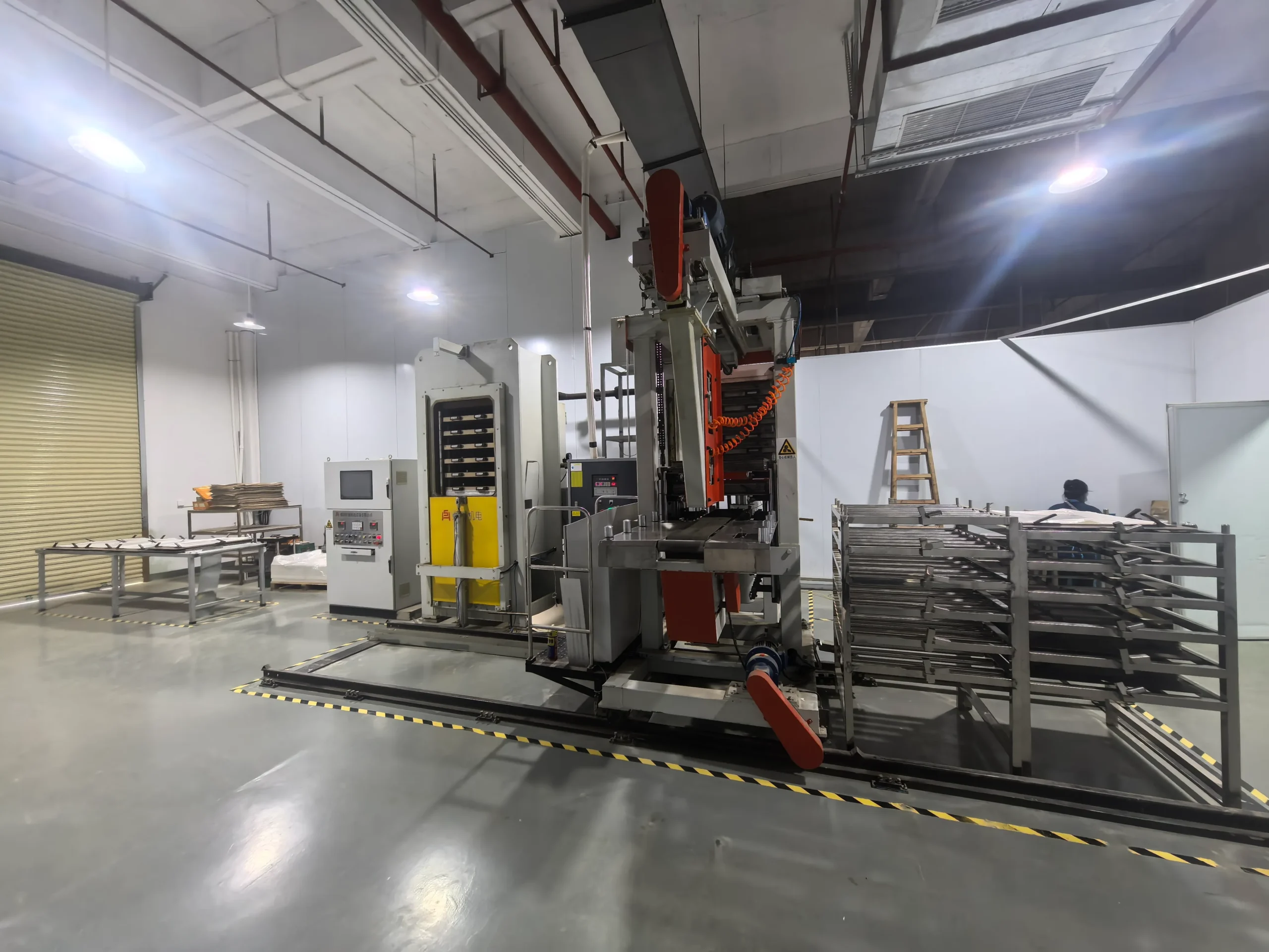
Laminating Machine
Multilayer lamination bonds the reviewed stack-up under controlled conditions to support structural stability, registration and long-term board reliability.

Drilling Machine
Precision drilling supports plated through-holes, vias, component holes and alignment across multilayer structures.

CNC Machine
CNC routing produces the required board outline, slots, cutouts and mechanical features for accurate installation in your product.

V-Cut Machine
V-cut processing supports efficient panel handling and controlled board separation during your assembly process.
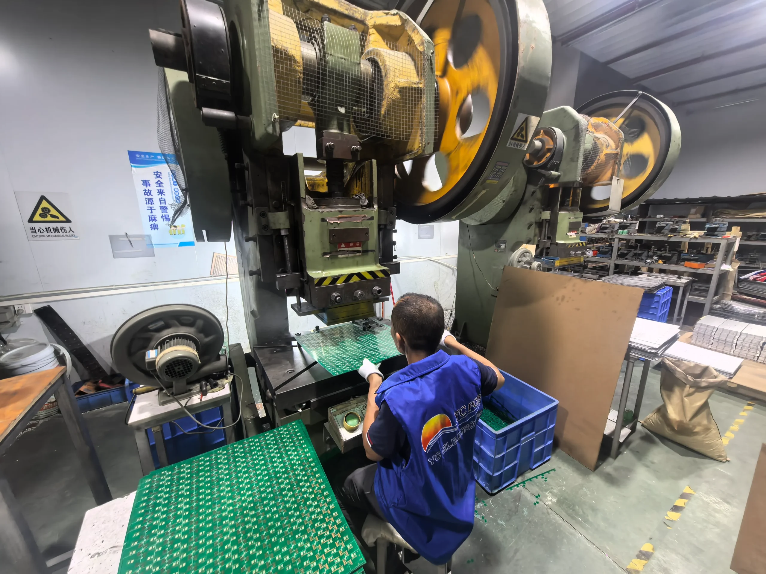
Die Punching Machine
Die punching provides repeatable profile processing for suitable board shapes and higher-volume production requirements.

Mold and Tooling Area
Dedicated tooling helps maintain consistent board shape, hole position and mechanical features across repeat production batches.
Surface Finish, Marking and Final Board Test
Solder mask, marking and final testing support solderability, board identification, assembly accuracy and electrical acceptance before shipment.
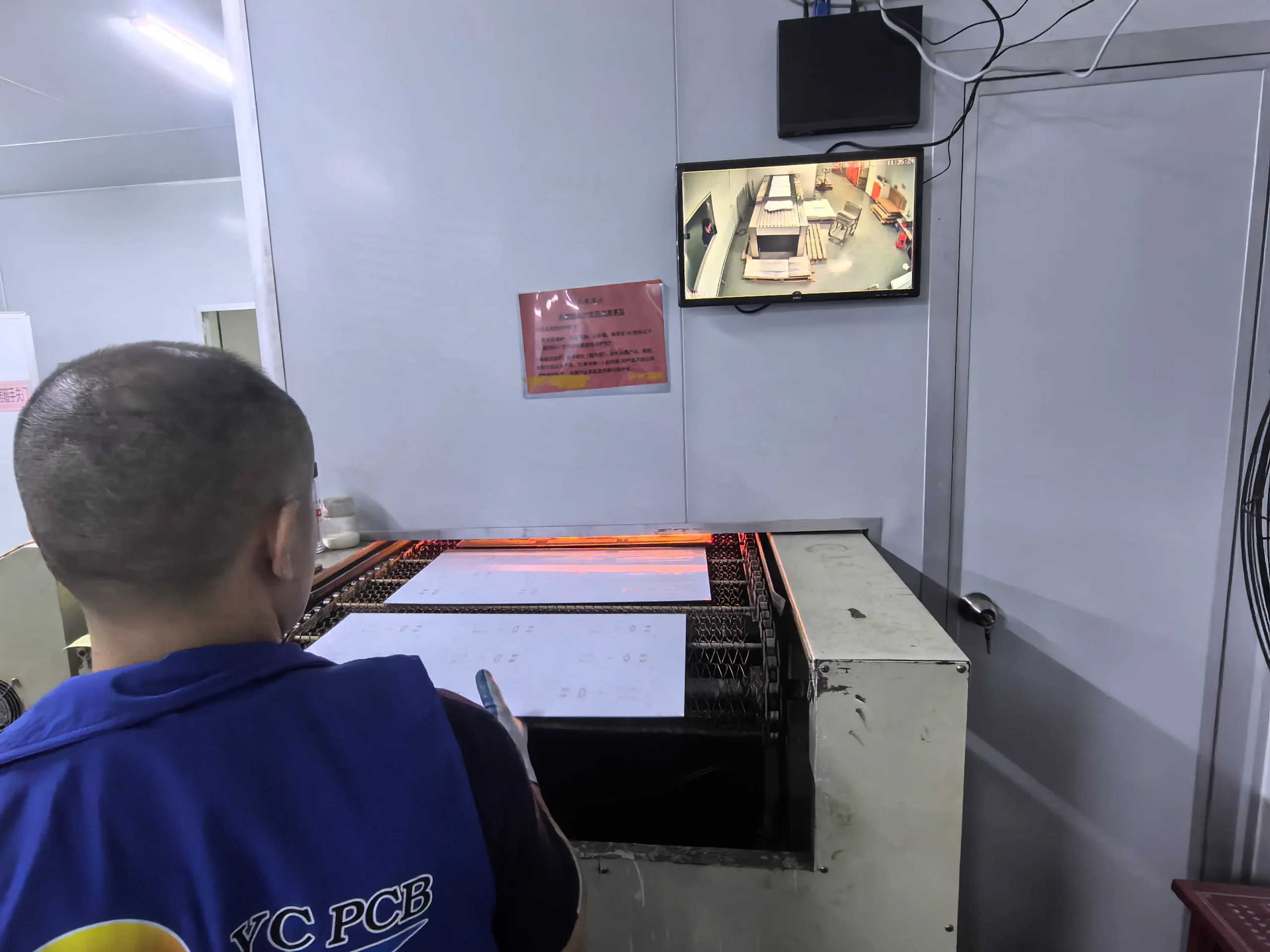
Solder Mask Line
Solder mask protects copper circuitry, defines solderable areas and supports cleaner, more reliable PCB assembly.
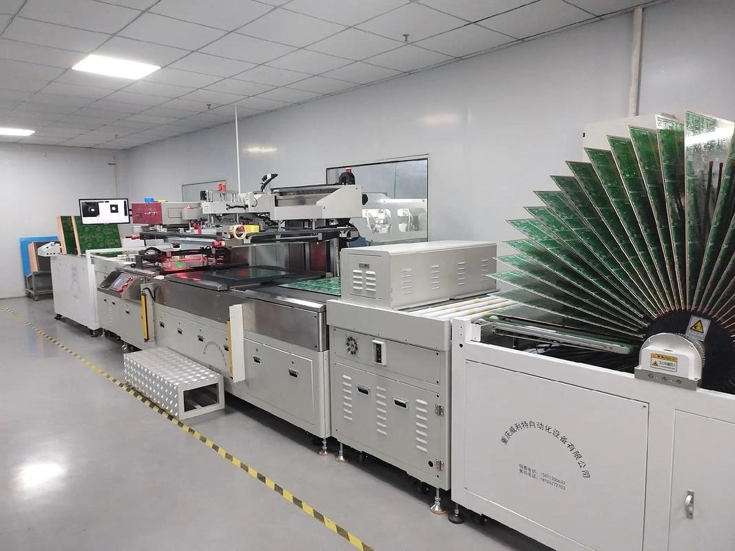
Silkscreen Process
Silkscreen can include component references, polarity marks, logos, revision information and assembly instructions according to your files.
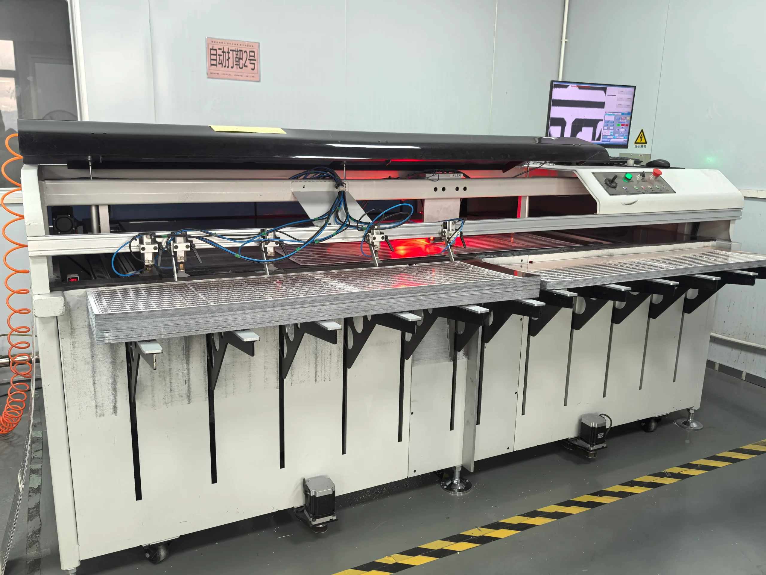
Automatic Shooting Machine
Automated process equipment helps improve handling consistency and maintain a stable production flow for repeat orders.

Automatic Testing Machine
Electrical testing verifies circuit continuity and isolation before shipment, helping reduce the risk of open and short circuits in assembly.
From PCB Files to Tested Boards
Your files move through a defined production and inspection route, making it easier to control manufacturability, quality checkpoints and delivery requirements from quotation to shipment.
File Review
Gerber files, drill data, stack-up and special notes are reviewed before production to identify manufacturability risks and confirm the correct process route.
Material Prep
Laminate and copper materials are selected according to your board thickness, copper weight, stack-up and application requirements.
Cutting & Cleaning
Panels are cut, cleaned and prepared to support stable registration through imaging, drilling and routing.
Imaging & Etching
Circuit patterns are transferred, etched and inspected to confirm traces, pads, spacing and copper features.
AOI Gate
AOI identifies circuit-pattern defects early, reducing the risk of defective panels moving into later production stages.
Lamination
Multilayer boards are laminated according to the approved stack-up, material system and production parameters.
Drilling
Vias, plated through-holes and component holes are drilled according to your drill files and tolerance requirements.
Solder Mask
Solder mask and surface preparation protect the circuitry and prepare the board for reliable component assembly.
Routing
CNC routing, V-cut or dedicated tooling produces the final board outline and mechanical features specified in your drawings.
Testing
Electrical testing, visual inspection, quantity confirmation and packing review are completed before shipment.
Inspection Points Across PCB Production
Quality control is integrated into material preparation, circuit formation, final bare-board testing and PCBA inspection. The inspection route can be matched to your board type, package selection and application risk.
Incoming Material Check
Material type, board thickness, copper weight and production requirements are checked before panels enter manufacturing.
AOI Pattern Inspection
AOI identifies open circuits, shorts, missing copper and pattern deviations before additional processing.

High-Voltage Testing
Withstand-voltage testing can be arranged for applicable projects to verify insulation performance and reduce electrical failure risk before shipment.
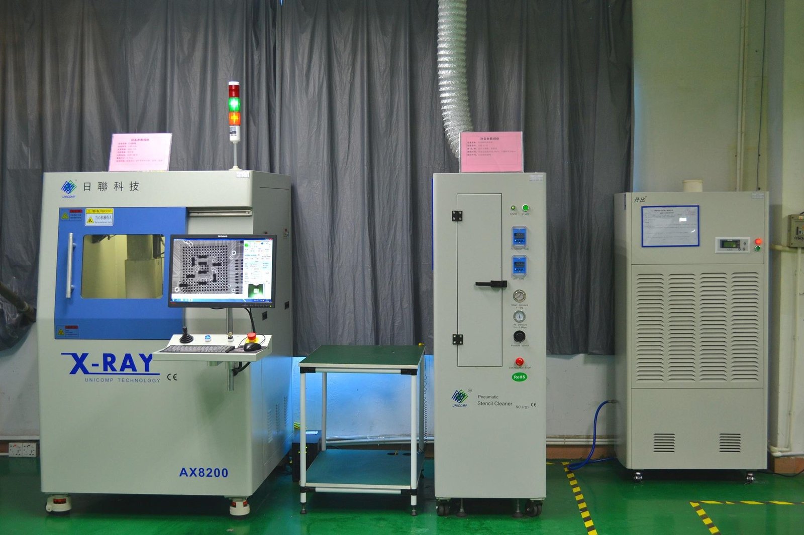
X-Ray Inspection
X-ray inspection can verify hidden solder joints beneath BGA, QFN and similar packages that cannot be fully assessed through visual inspection alone.
Integrated PCB Assembly and Verification Capabilities
Choose bare PCB fabrication or extend the project to component sourcing, SMT, DIP, programming, functional testing and full product assembly. An integrated route reduces supplier handoffs and helps keep fabrication and assembly requirements aligned.
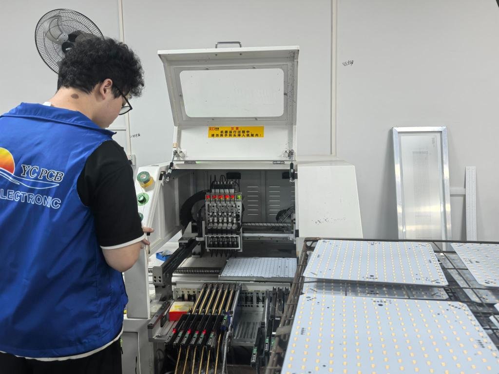
SMT Production Workshop
Our SMT workshop supports solder paste printing, automated placement, reflow soldering and inspection for prototype, pilot-run and batch PCBA orders.
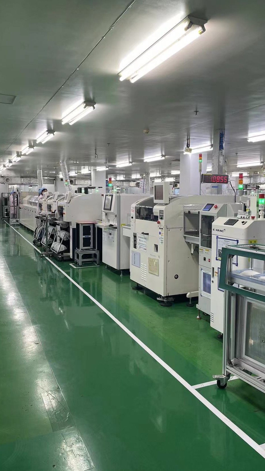
SMT Placement Machine
Automated placement equipment supports repeatable component positioning after BOM review, feeder setup and program verification.
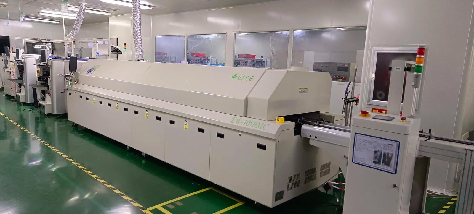
Reflow Soldering
Controlled reflow profiles support consistent SMT solder joints and can be adjusted for temperature-sensitive components and mixed package requirements.
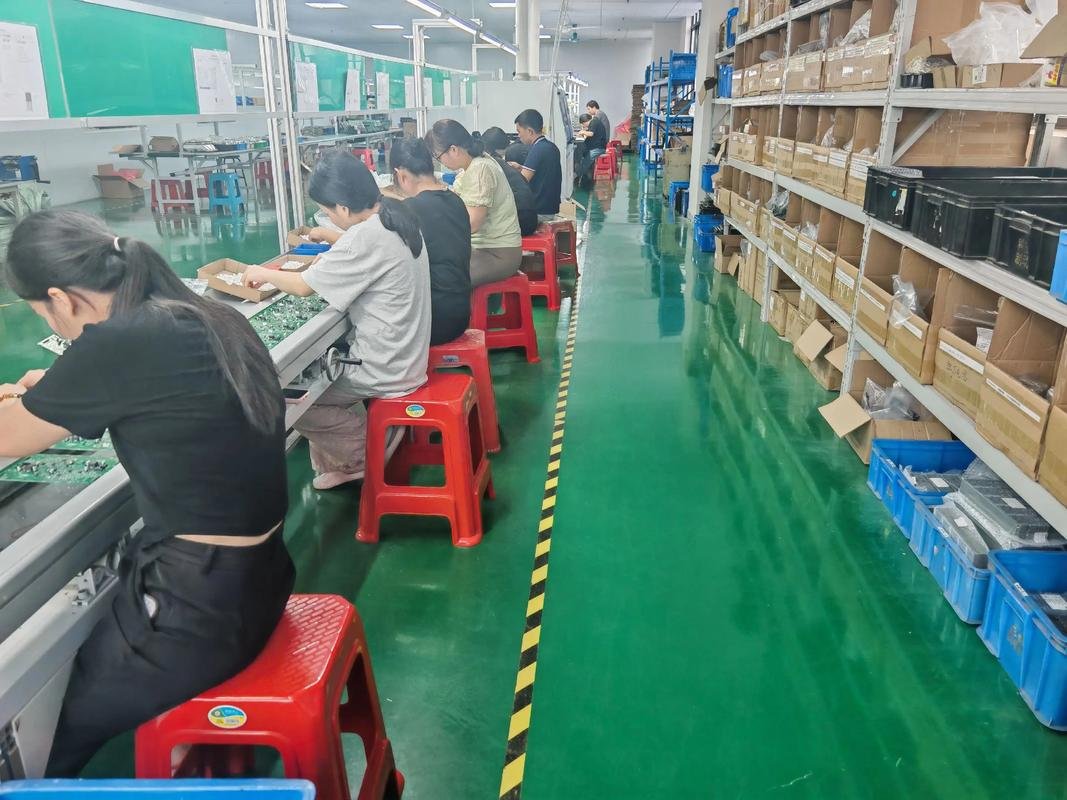
DIP Component Insertion
DIP insertion supports connectors, transformers and larger components that require mechanical strength or mixed SMT and through-hole assembly.
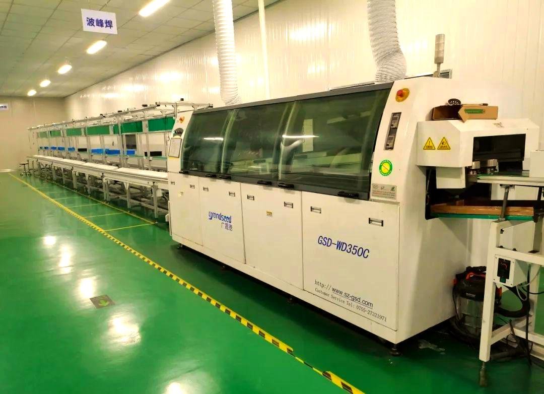
Wave Soldering Line
Wave soldering supports efficient through-hole assembly after component orientation, masking and soldering parameters are confirmed.
X-Ray Verification
X-ray verification helps inspect hidden joints in complex packages and supports quality control for demanding PCBA projects.
Why Procurement Teams Work with YC PCB
Qualify your PCB supplier based on visible production resources, controlled manufacturing processes and inspection readiness—not quotation price alone. YC PCB supports technical review from files and materials through testing, packing and shipment.
Visible Manufacturing Resources
- Actual production equipment and workshop areas can be reviewed.
- Key fabrication, assembly and inspection areas follow defined process stages.
- Factory equipment and process photos can support capability confirmation.
- Prototype, pilot-run and batch orders follow a project-specific production route.
Process Control
- Material, cutting, imaging, drilling and routing requirements are reviewed before production.
- Multilayer stack-ups are checked against project files before lamination.
- Slots, V-cuts, cutouts and board outlines are produced according to mechanical drawings.
- Special materials, tolerances, testing and packing requirements can be confirmed before production.
Inspection and Shipment Control
- AOI is used to identify circuit-pattern defects during production.
- Electrical testing is completed before bare PCB shipment.
- PCBA inspection and functional testing can be planned according to project requirements.
- Packing, labels, quantity and shipping requirements are confirmed before delivery.
PCB Factory and Production FAQ
Review the information below before sending your files. It explains what we need to confirm materials, production route, inspection requirements and delivery planning.
What manufacturing information can YC PCB provide before an order?
We can provide information on production equipment, manufacturing flow, inspection methods and available project evidence so your procurement and engineering teams can evaluate the production route before ordering.
What files and specifications should I send for review?
Please send Gerber files, drill files, stack-up, copper weight, board thickness, surface finish, quantity, tolerance notes and any assembly or testing requirements. A BOM and pick-and-place file are also needed for PCBA projects.
How is PCB quality controlled during production?
Quality is controlled through material verification, imaging, etching, lamination, drilling, solder mask, routing, AOI and electrical testing. For PCBA projects, BOM control, component placement, soldering and functional testing are added to the inspection route.
Can YC PCB support prototypes and repeat production?
Yes. We support prototype, pilot-run and batch production, with the process route reviewed according to your files, quantity, delivery needs and manufacturing requirements.
Can I request production and inspection records?
Production photos, order-status updates, packing photos and applicable test records can be discussed according to the order type and your documentation requirements.
Can YC PCB review both bare PCB and PCBA requirements?
Yes. We can review bare PCB fabrication, component sourcing, SMT and DIP assembly, programming, inspection, functional testing and packing requirements as part of one project.
Send Your PCB Files for a Manufacturing Review
Send your Gerber files, stack-up, quantity and target application for a manufacturing review. Our team will check the proposed production route, material requirements, inspection needs and PCBA scope before preparing the quotation.
Project-Specific Inspection Before Shipment
Your project can be linked to defined production checkpoints, electrical testing, X-ray inspection for applicable assemblies, packing confirmation and shipment records.
Send Your PCB Requirements
Share your contact details and project requirements. You may include the PCB type, layer count, quantity, material, surface finish, testing needs and target delivery time.
 English
  Japanese
  French
  German
  Spanish
  Italian
  Portuguese
  Russian
  Dutch
Dutch  Turkish