
Server and Data Center PCB Manufacturing Solutions
Source high-layer-count server PCBs and assembled boards from one manufacturing partner. YC PCB supports server motherboards, storage backplanes, network equipment, AI accelerator boards and power boards with stack-up, impedance, low-loss material, back-drilling, HDI, thermal and PCBA process support.
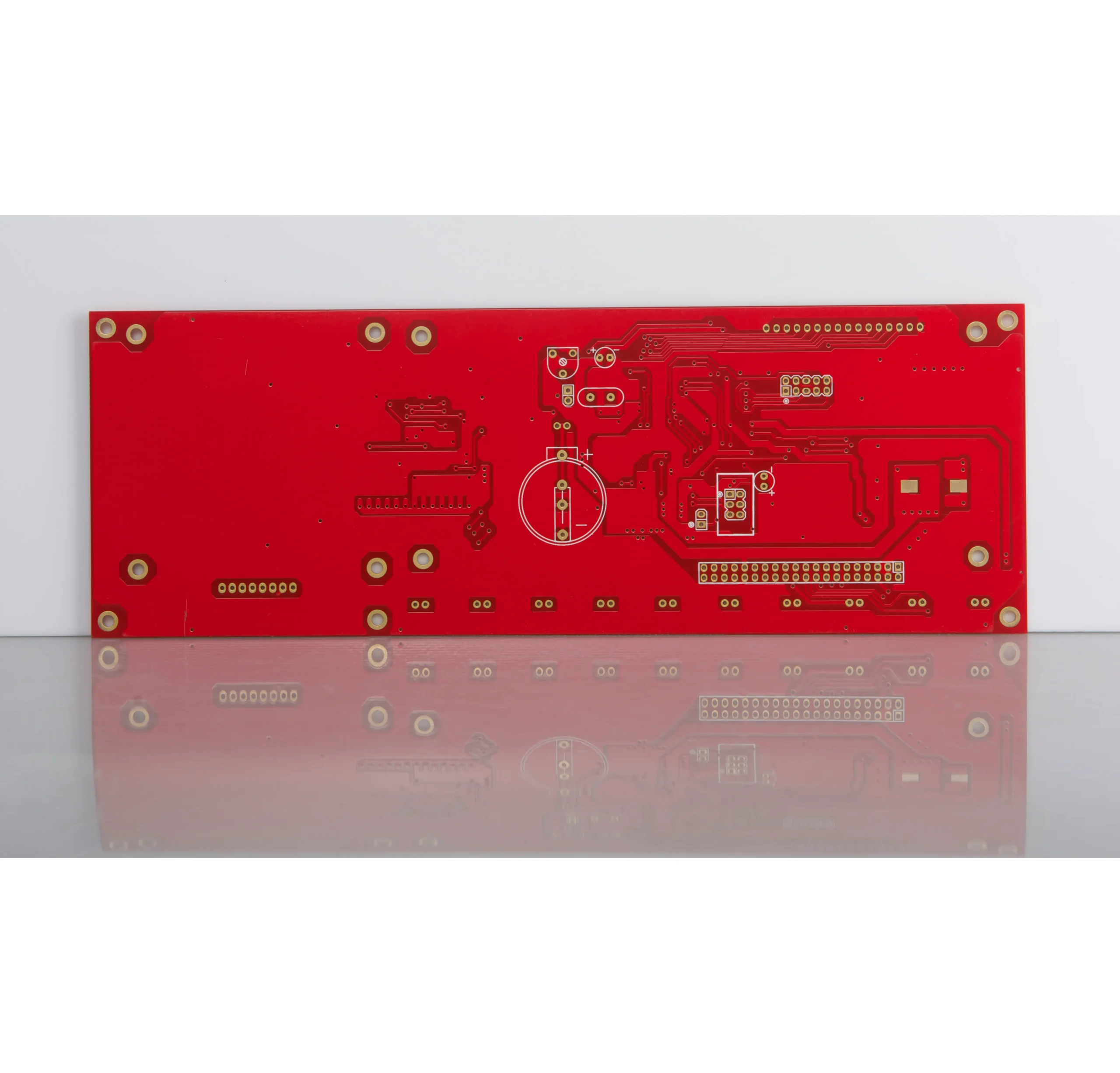
Multilayer capability for complex server and networking projects
Blind vias, buried vias and dense BGA routing after file review
SMT, BGA, X-Ray, ICT and FCT from bare board to assembly
Manufacturability review before production to reduce prototype risk
Reliable Server Hardware Starts with the Right PCB
Server and data center hardware places demanding requirements on signal integrity, power delivery, thermal management and board flatness. YC PCB coordinates material, stack-up, impedance, via structure and assembly details so your boards are prepared for continuous operation and repeat production.
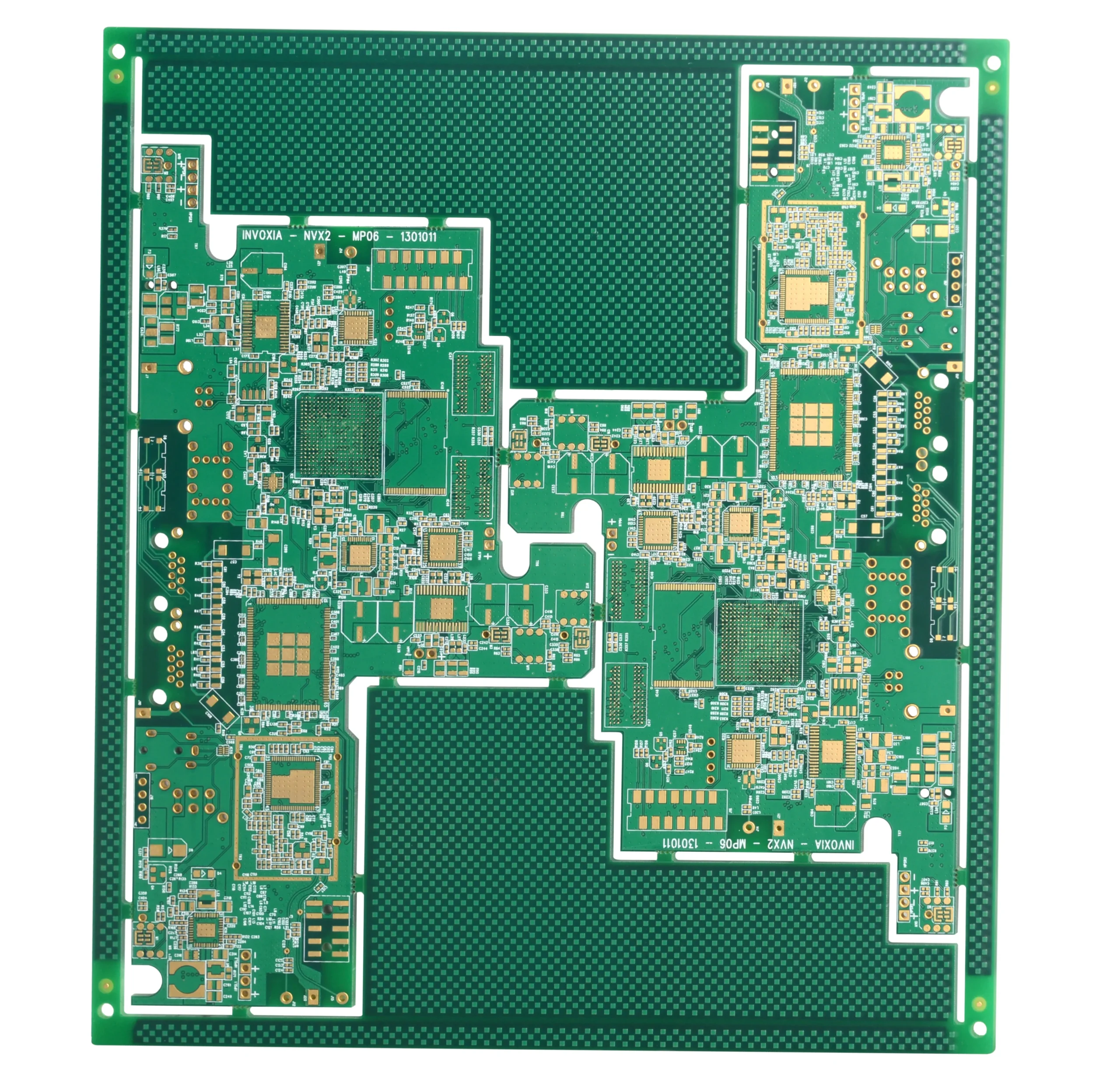
Protect Signal Margin and Assembly Yield
Early confirmation of stack-up, via stubs, copper balance, thermal paths and BGA assembly details helps reduce redesigns, warpage, soldering defects and delayed validation.
Solutions for Server, Storage, Network and AI Hardware
Send your design files, quantity and delivery target. Our engineering team will recommend a practical manufacturing route based on layer count, interface speed, BGA density, copper weight, material requirements, connector design and test scope.
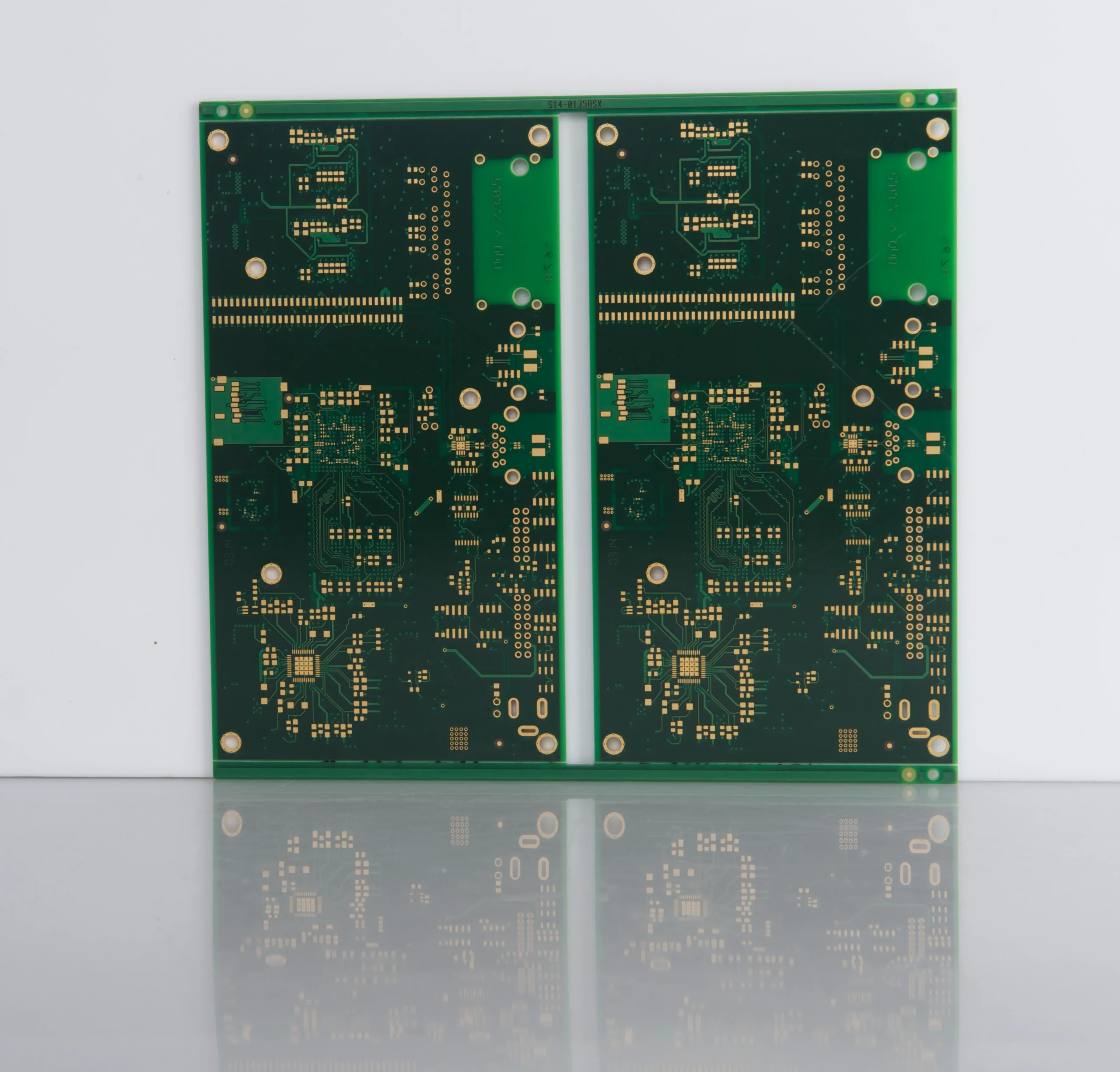
Server Motherboard PCB
High-layer-count motherboards for CPU, memory and VRM sections, with controlled stack-up, dense BGA routing and balanced copper.
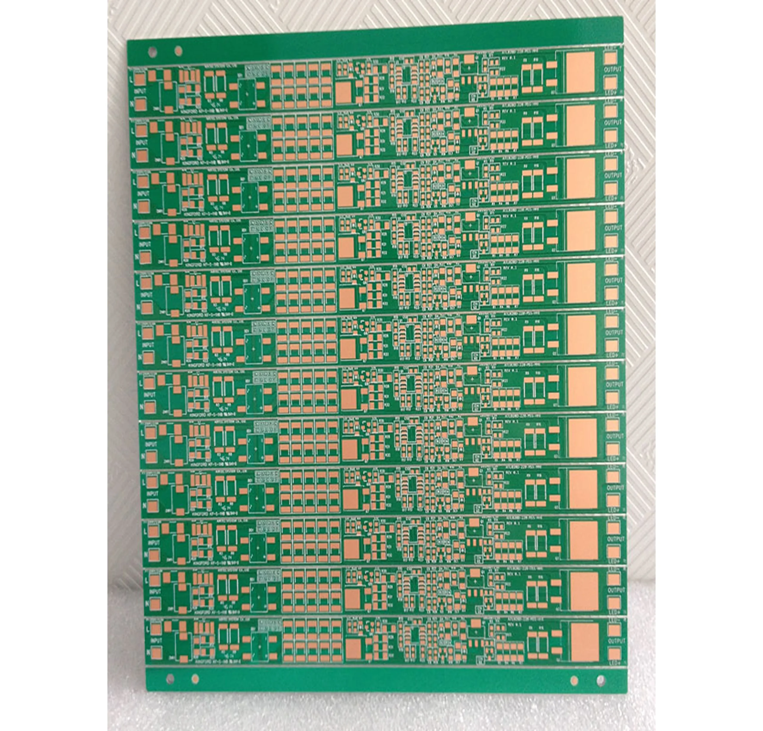
High-Speed Network Board
Controlled-impedance boards for switches, routers and optical network equipment, with low-loss material and signal-path support when required.
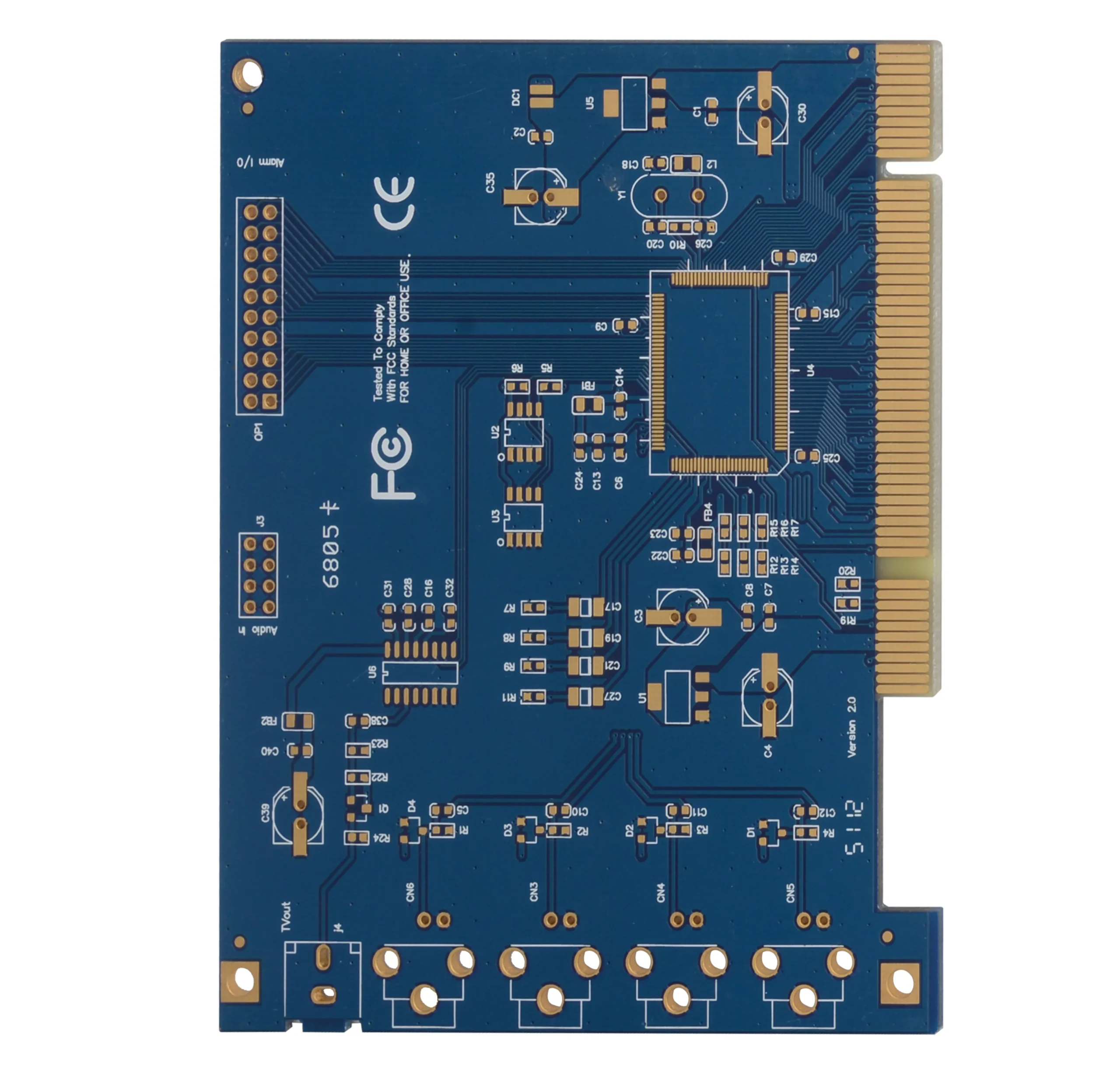
Storage Backplane PCB
Connector-dense backplanes for PCIe, NVMe and storage expansion, with back-drilling, mechanical fit and lane consistency support.

Power Distribution Board
Heavy-copper and power boards designed around current paths, thermal vias, copper thickness and heat-spreading requirements.

AI Accelerator PCB
HDI and multilayer boards for accelerator and GPU-related hardware, supporting dense routing, high current and thermal management requirements.
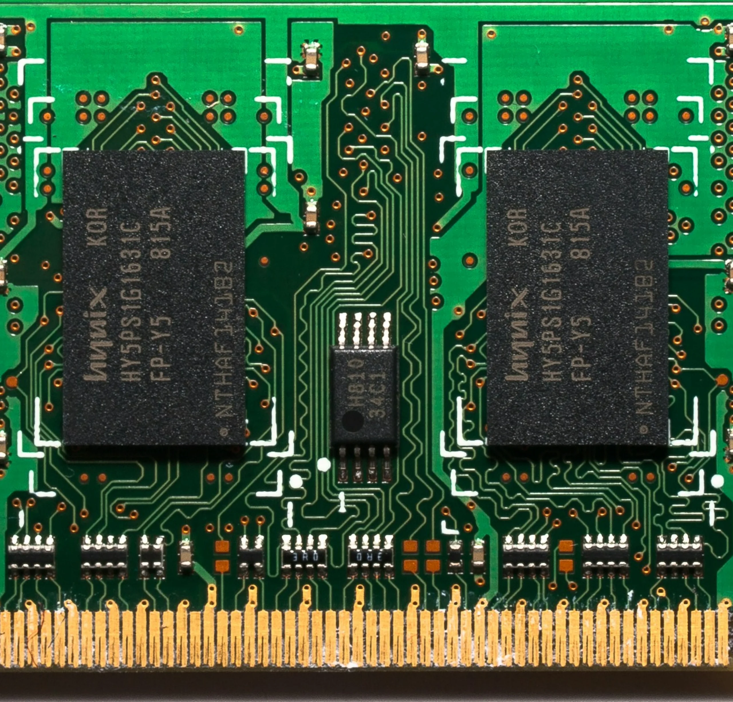
Data Center PCBA
Turnkey assembly for server and network boards, including component sourcing, SMT/BGA placement, X-Ray, ICT, FCT and project-specific packing.
Key Items We Confirm for High-Speed Server PCB Orders
Before production, our engineers confirm the details that influence performance, manufacturability and repeatability. This gives your purchasing and engineering teams a clearer build route before material and tooling are committed.
Material Selection
We match standard FR4 or low-loss material options to your interface speed, channel length, Dk/Df target, operating environment and budget.
Stack-Up & Reference Planes
We review layer order, dielectric thickness, reference planes, ground continuity and stack-up symmetry to support controlled routing and reduce warpage risk.
Differential Impedance
Provide single-ended and differential impedance values, tolerances and critical net groups. We confirm manufacturable trace geometry, coupon design and TDR reporting needs.
Via Structure & Back-Drilling
Back-drilling, blind or buried vias, via-in-pad and HDI structures are evaluated where dense BGA fanout or high-speed channels require them.
Power Delivery & Copper Balance
We check copper weight, power planes, current paths, decoupling areas and copper distribution for stable power delivery and repeatable fabrication.
BGA & QFN Assembly
Pad design, solder mask openings, stencil, reflow profile and X-Ray requirements are confirmed to improve BGA and QFN assembly yield.
Select the Right Stack-Up and Material for Your Project
Share the following information with your RFQ so we can recommend the right material and build route without adding unnecessary cost. Final specifications are confirmed after your speed target, drilling plan, BGA layout and assembly scope are reviewed.
| Design Area | What Your Project Needs | YC PCB Manufacturing Support |
|---|---|---|
| Layer Count | Enough signal, power and ground layers to support memory, storage, network, control and power-delivery functions. | Layer-count feasibility, lamination sequence, copper balance, drill structure and production panel planning. |
| Low-Loss Material | Suitable dielectric performance for long differential pairs, SerDes links and other loss-sensitive channels. | Material family, Dk/Df target, signal-layer position, channel length and cost-effective alternatives. |
| Impedance Control | Predictable trace geometry and reference planes for PCIe, SerDes, Ethernet, memory and other controlled-impedance nets. | Impedance values, trace geometry, dielectric thickness, test coupons and TDR report requirements. |
| Back-Drilling / HDI | A via structure that supports dense BGA breakout while limiting unwanted stubs on critical signal paths. | Back-drill depth, residual-stub target, blind/buried vias, via-in-pad filling and plating process. |
| PDN and Heavy Copper | Low-resistance current paths and effective heat spreading around VRM, processor and power-module areas. | Copper weight, plane geometry, thermal-via areas, heat-source locations and current-path requirements. |
| Data Center PCBA | A controlled assembly and test route for dense BGAs, high-pin-count connectors and functional interfaces. | BOM, pick-and-place data, package details, X-Ray scope, ICT/FCT fixtures and ESD packing requirements. |
A Clear Route from Engineering Review to Tested PCBA
One team coordinates PCB fabrication, component sourcing, assembly, inspection and packing, reducing supplier handoffs and making prototype-to-batch production easier to manage.
File & Requirement Review
We check Gerber or ODB++, drill files, stack-up, impedance requirements, mechanical drawings, quantities and target delivery dates.
DFM & Stack-Up Confirmation
Our engineers confirm layer order, dielectric thickness, reference planes, copper balance, via structure and any back-drilling requirements.
PCB Fabrication
Boards are manufactured using the confirmed material, lamination, drilling, plating, solder mask and surface-finish process.
Electrical & Impedance Testing
Electrical testing and impedance-coupon verification are completed according to the agreed inspection and documentation requirements.
SMT / BGA Assembly
SMT, BGA/QFN reflow, connector soldering and X-Ray inspection are carried out according to the approved assembly route.
Functional Test & Packing
ICT/FCT fixtures, firmware steps, ESD protection, board support, labels and delivery documents are completed as specified.
Critical Checks That Protect Your Server PCB Order
These checks help reduce signal loss, soldering defects, warpage, hot spots and test delays before your boards reach system validation.
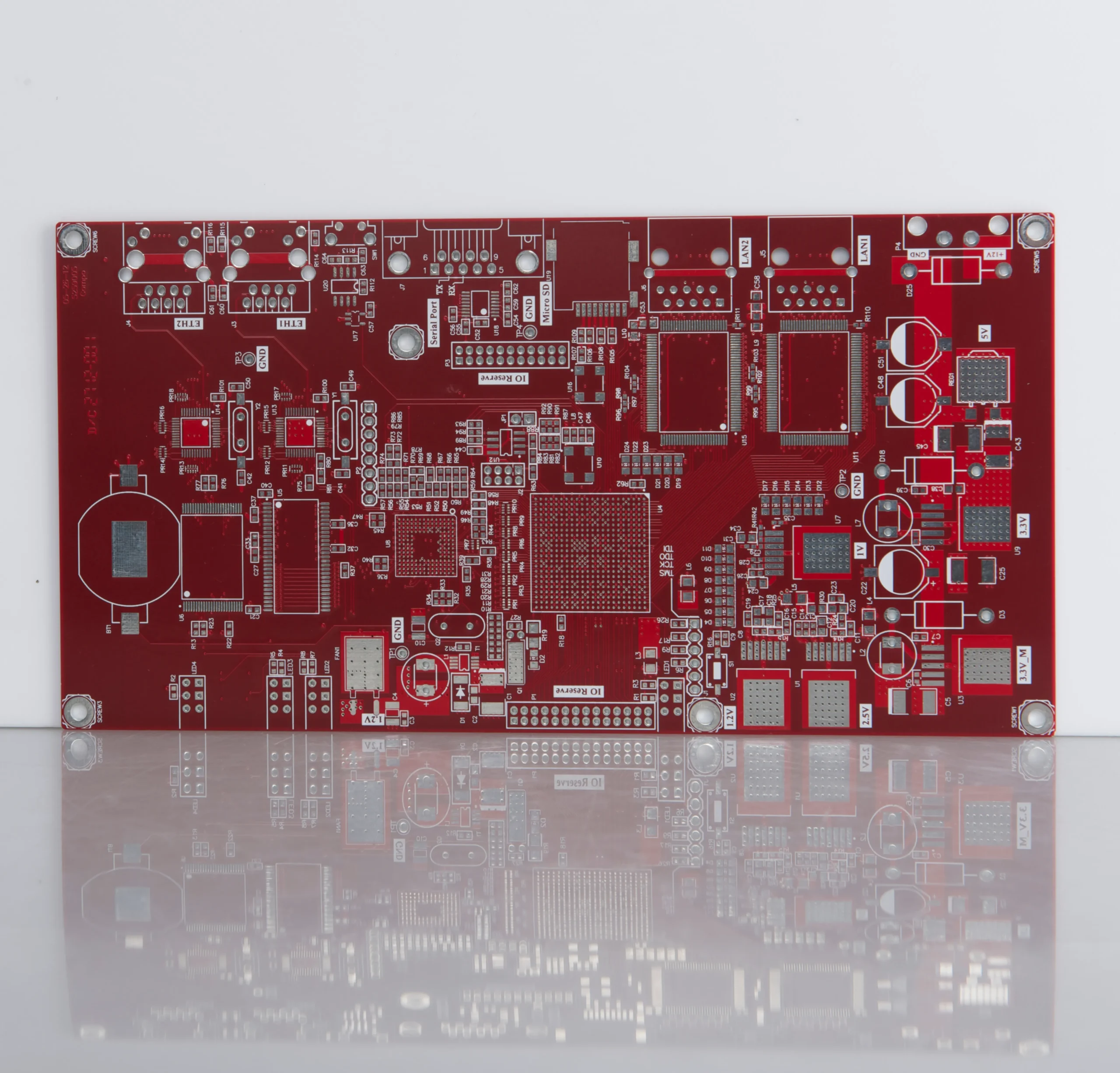
Impedance Coupon
Critical channels, coupon design and TDR reporting requirements are confirmed before fabrication begins.
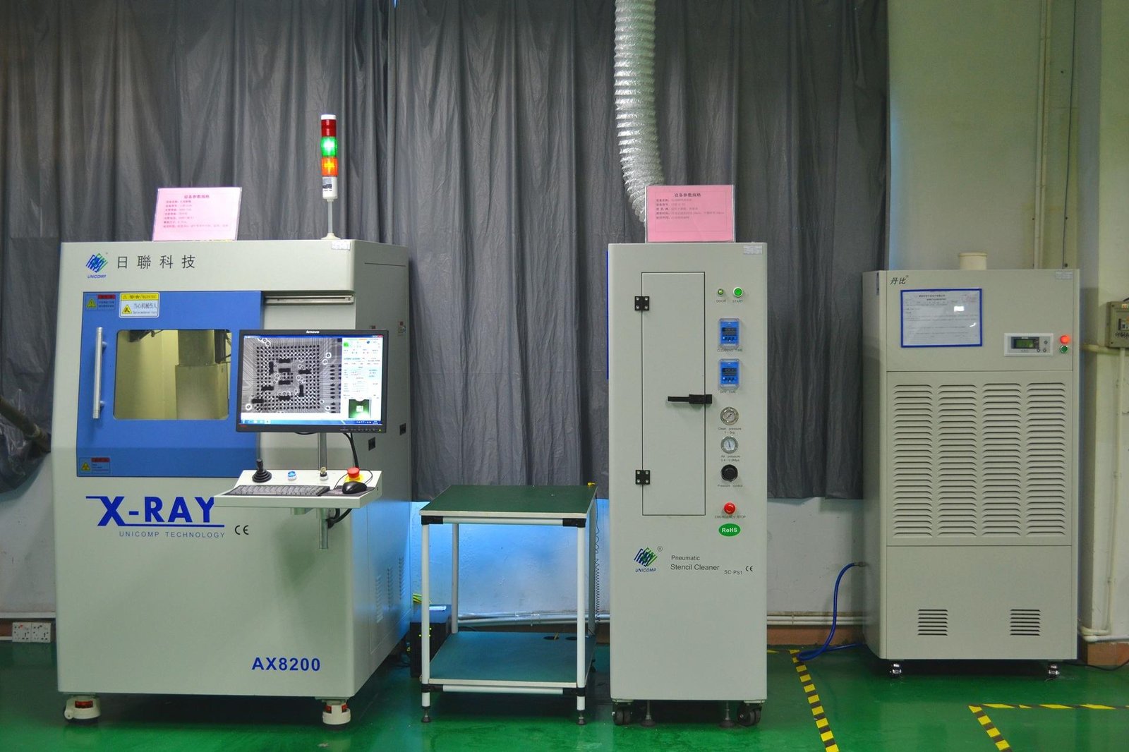
BGA X-Ray
X-Ray inspection verifies hidden solder joints beneath BGA and QFN packages that cannot be checked visually.
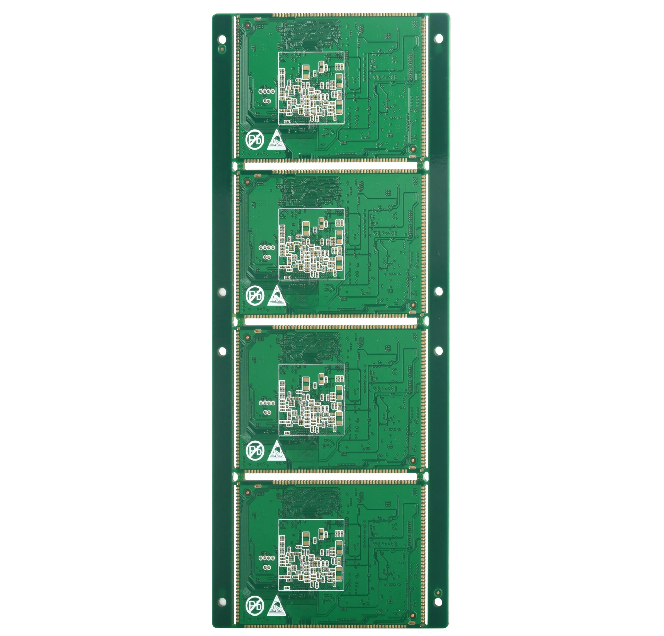
Thermal Path
Heat-source locations, copper planes, thermal vias and contact areas are coordinated to improve heat spreading.

Copper Balance
Balanced copper distribution and a suitable lamination route help reduce warpage in high-layer-count boards.
PCB and PCBA for Data Center Hardware
YC PCB supports bare-board and assembled solutions for computing, storage, networking, power, management and validation hardware.
Cloud Server Boards
High-layer-count PCB and PCBA for cloud infrastructure, rack servers and dense computing platforms.
AI Accelerator Hardware
HDI and multilayer PCB support for accelerator modules, GPU-related boards and high-power computing electronics.
Storage Backplanes
Connector-heavy storage, NVMe and expansion boards with mechanical-fit, back-drilling and high-speed lane support.
Network Equipment
Controlled-impedance PCB and PCBA for switches, routers, optical networking and communication equipment.
Edge Computing Systems
Compact boards manufactured around enclosure space, thermal paths, connector positions and environmental requirements.
Power and VRM Boards
Heavy-copper and power-distribution boards matched to current, temperature-rise and heat-spreading requirements.
Management Modules
Control, monitoring, interface and BMC-related boards for server and data center equipment.
Test and Validation Boards
Fixture boards, interface boards and validation PCBA for engineering tests and production verification.
Send Your Files for a Server PCB or PCBA Quote
Share your design package, target quantity and delivery requirement. We will confirm the manufacturing route, raise any technical questions and prepare the quotation.
Start Your Server PCB Project
Open the project form and send your contact details together with the board type, layer count, quantity, material, impedance, delivery target and PCBA requirements.
Server Data Center PCB FAQ
Answers to common questions from purchasing managers and hardware engineers preparing server PCB, network board and data center PCBA orders.
What makes a server PCB different from a standard multilayer PCB?
A server PCB usually carries high-speed channels, dense BGA routing, multiple power domains, strict impedance requirements and higher thermal load. Stack-up, material loss, via design and PDN planning must be reviewed together.
What files should be sent for high speed server PCB review?
Send Gerber or ODB++ data, drill files, stack-up notes, impedance table, material preference, copper weight, BGA pitch, back-drilling notes, mechanical drawing, BOM and test requirements if assembly is needed.
Can YC PCB review high-layer-count data center circuit boards?
YC PCB can review high-layer-count PCB projects according to stack-up, material, drill, impedance, copper balance, BGA routing and testing requirements. The final route is confirmed after file review.
When should low-loss materials be considered for data center boards?
Low-loss materials should be considered when the design includes high-speed interfaces, long differential pairs, SerDes channels, high-frequency networking paths or signal margin requirements that cannot be met with standard FR4.
Why is back-drilling used in high speed server PCB designs?
Back-drilling helps remove unused via stubs that can create reflections and degrade high-speed signals. It is commonly reviewed for PCIe, SerDes, high-speed network and storage interface designs.
Can YC PCB support data center PCBA assembly?
YC PCB can review data center PCBA projects involving SMT, BGA, QFN, component sourcing, AOI, X-Ray, ICT, FCT and project-specific functional testing requirements.
How should PDN and thermal requirements be described?
Provide power rails, current areas, VRM position, copper weight, heat source locations, thermal via needs, heat sink contact areas and any system cooling constraints so the design can be reviewed properly.
Is HDI required for server and AI computing boards?
HDI may be needed when BGA density, routing escape, connector pitch or board size limits cannot be handled with standard through-hole multilayer routing. The need should be confirmed through stack-up and layout review.
How does copper balance affect high-layer-count server boards?
Uneven copper distribution can increase lamination, plating and reflow warpage risk. High-layer-count server boards should be reviewed for symmetrical structure and balanced copper areas.
Can YC PCB support network equipment and 5G PCB projects?
Yes. We can support network and communication PCB projects with high-frequency materials, impedance control, thermal management, assembly and project-specific testing after file review.
Get a Manufacturing Route and Quote for Your Server PCB
Send your PCB files, stack-up, impedance table, quantity and PCBA requirements. YC PCB will confirm the material, via structure, inspection route and assembly scope needed for prototype or batch production.
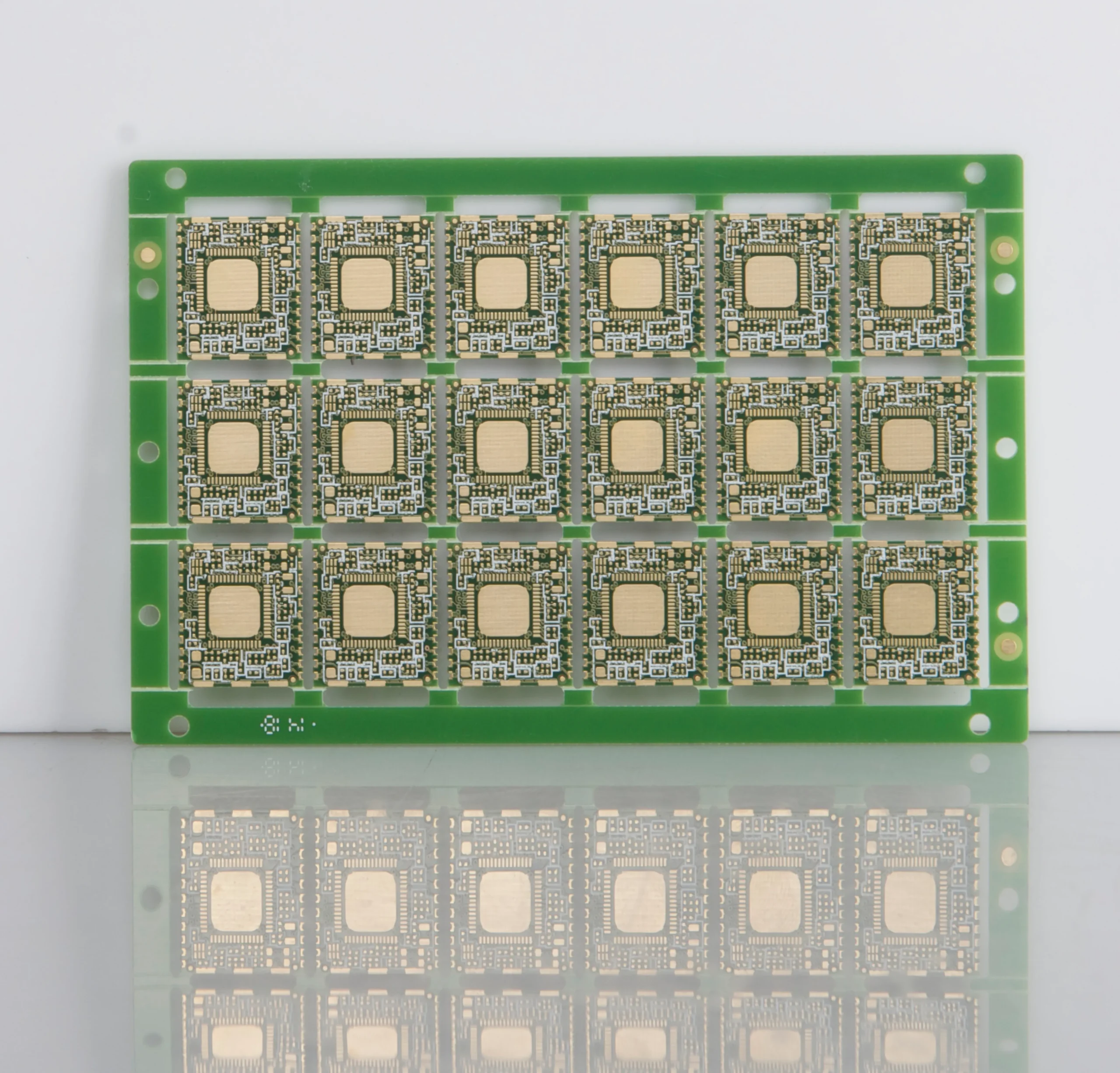
Reduce Risk Before the First Build
Early confirmation of stack-up, impedance, via design, copper balance, assembly and test requirements helps prevent avoidable redesigns and production delays.
Send Your Project Requirements
Tell us how to contact you and briefly describe your PCB or PCBA project. You may include the board type, layer count, quantity, material, impedance, delivery target and assembly requirements.
 English
  Japanese
  French
  German
  Spanish
  Italian
  Portuguese
  Russian
  Dutch
Dutch  Turkish