 Skip to content
20 Layer FR4 HDI PCB
YC PCB manufactures 20 layer FR4 HDI PCBs for advanced electronics requiring dense BGA routing, multiple signal and reference planes, controlled impedance and compact interconnects. Bare PCB fabrication and optional PCBA are available from prototype through repeat production.
Available manufacturing options include high Tg FR4, blind and buried vias, microvias, via-in-pad, controlled impedance, ENIG and mixed SMT/THT assembly. Final build details are confirmed from your approved stack-up, drill data and assembly requirements.

Key HDI PCB Details
Confirm the required layer structure, BGA fan-out, HDI via type, impedance targets, material, surface finish and testing scope before ordering.
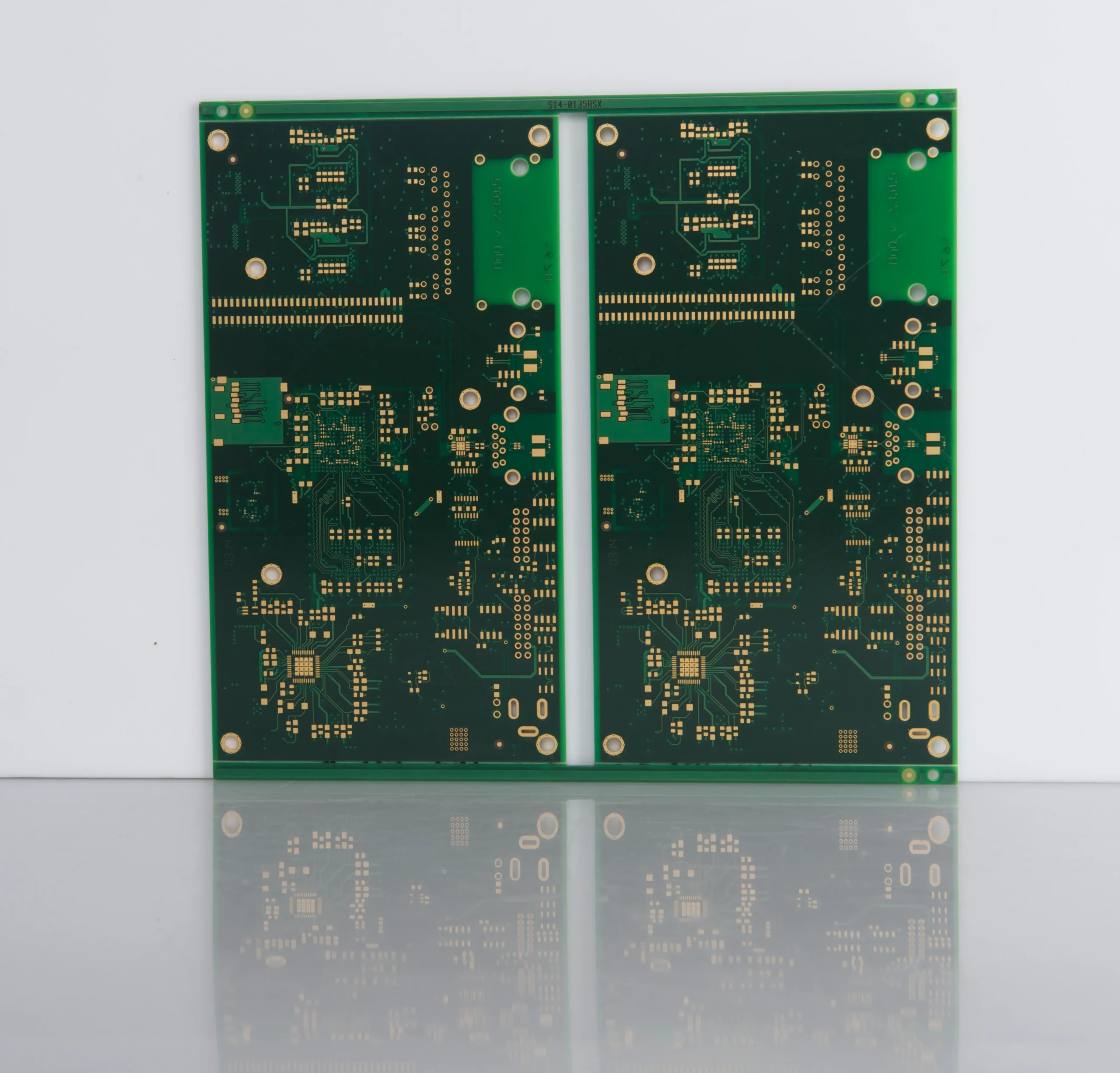
Dense BGA routing, microvias, ENIG pads and the mechanical outline are produced according to the approved fabrication data.

Signal, ground and power layers are assigned to support return paths, power distribution, impedance control and stack-up symmetry.
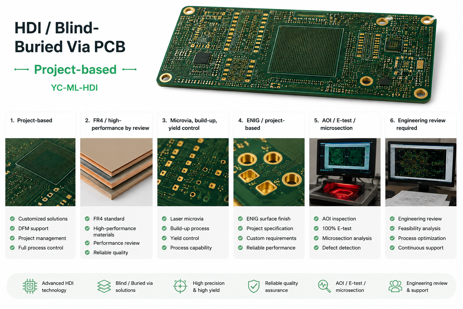
Microvia type, via-in-pad requirements, BGA pitch and fine-line spacing must be included in the fabrication and drill data.
What Is a 20 Layer FR4 HDI PCB?
A 20 layer FR4 HDI PCB is an advanced high density multilayer circuit board designed for projects that need more routing layers, compact interconnection, reference planes and higher design complexity than standard multilayer boards.
High Density Multilayer
Supports compact circuit layout, dense signal routing and multi-layer planning for advanced electronics.
HDI Via Review
Blind vias, buried vias, microvias and via-in-pad structures can be reviewed according to the submitted files.
Stack-Up Planning
Signal, ground and power layers should be reviewed together to reduce routing risk and support stable production.
20 Layer HDI PCB Product Details
Quotation accuracy depends on the complete L1-L20 stack-up, board outline, BGA fan-out, microvia structure, surface finish and impedance requirements.
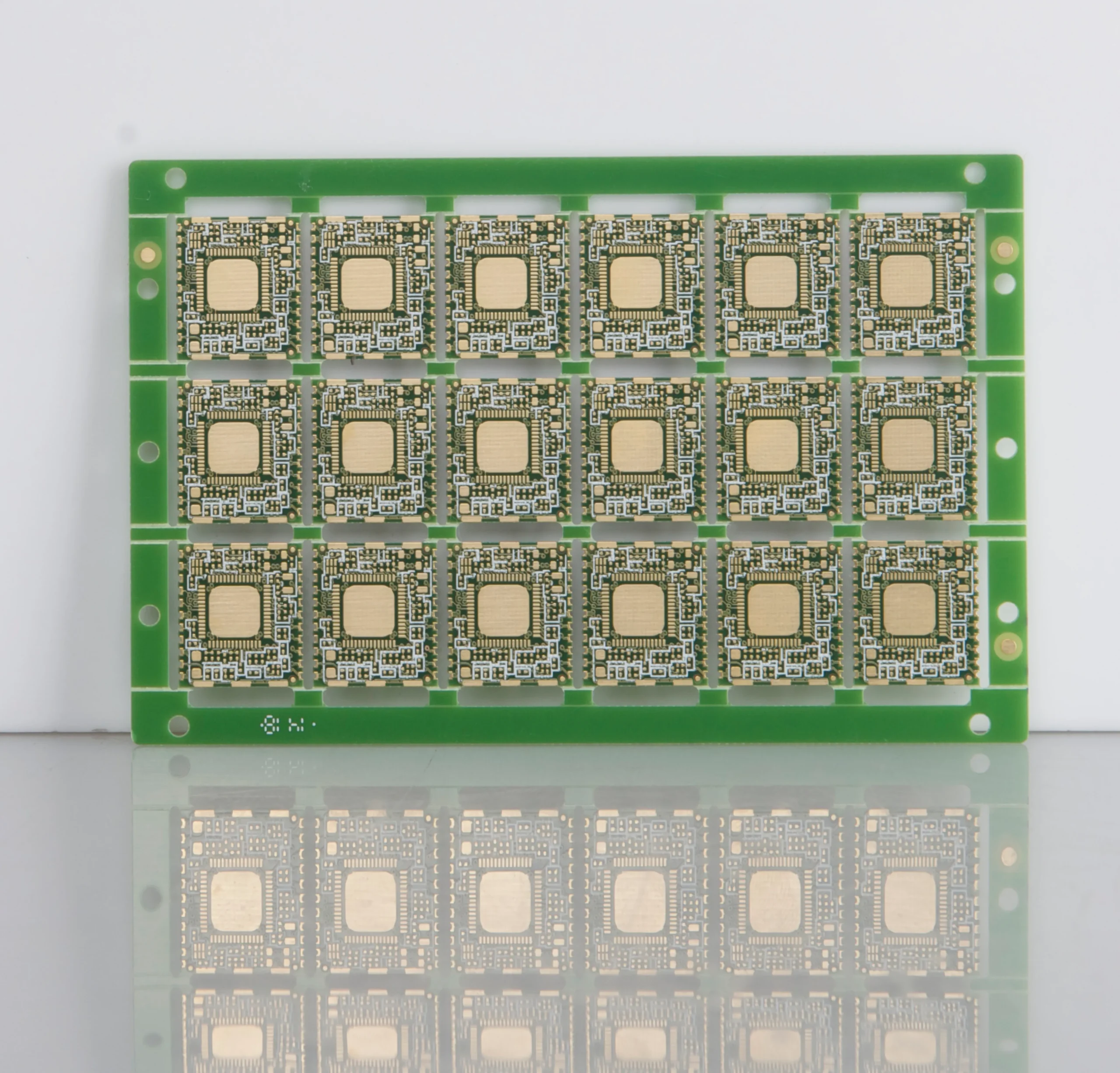
The finished board can include dense routing, custom mounting holes, ENIG pads and complex multilayer interconnections.
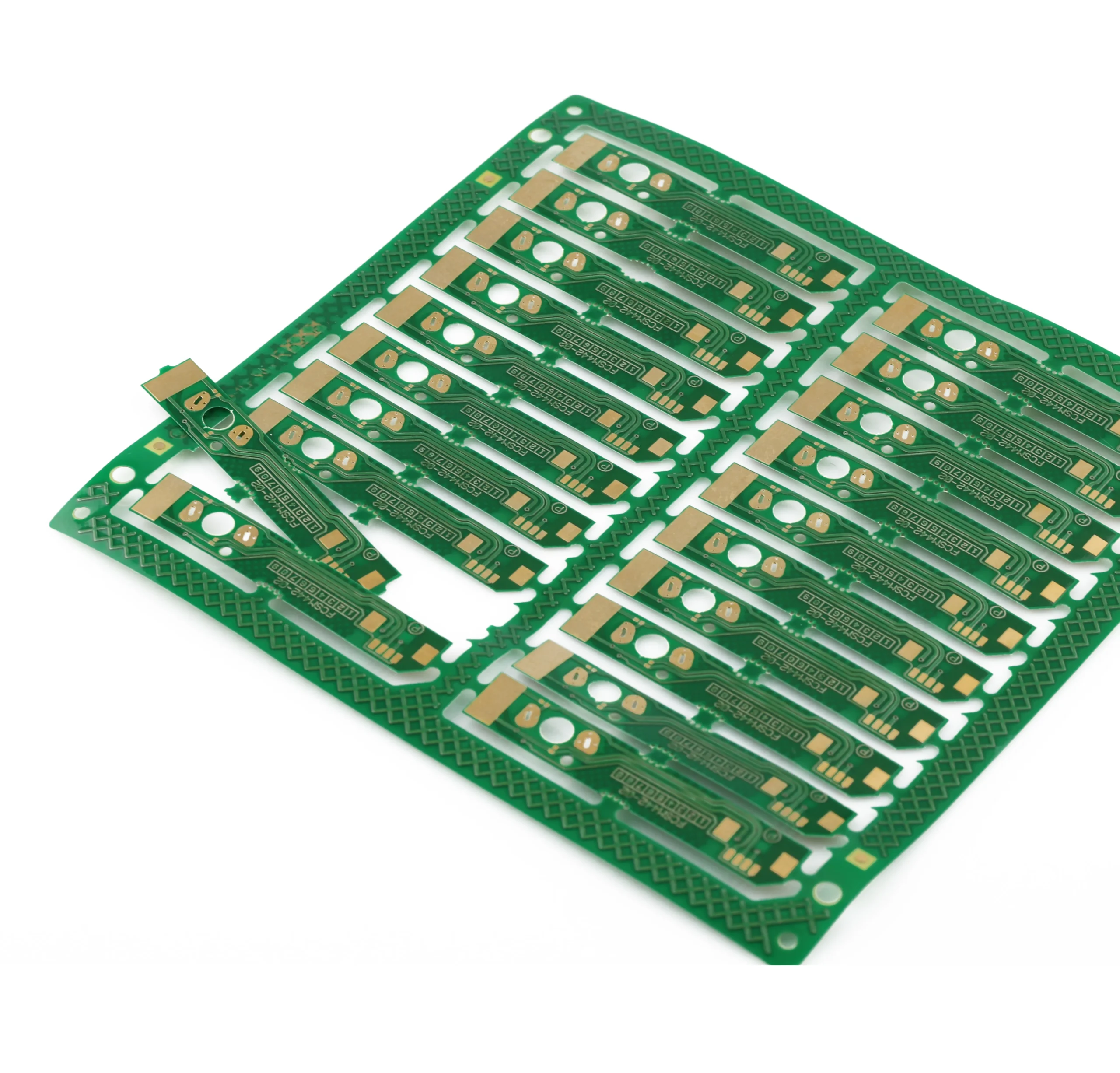
Supports microvias, via-in-pad, fine-pitch BGA escape routing and compact component layouts.
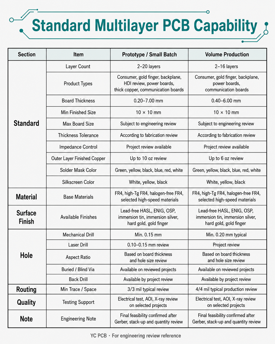
Layer assignment, dielectric spacing and copper balance determine impedance, reliability and finished board thickness.
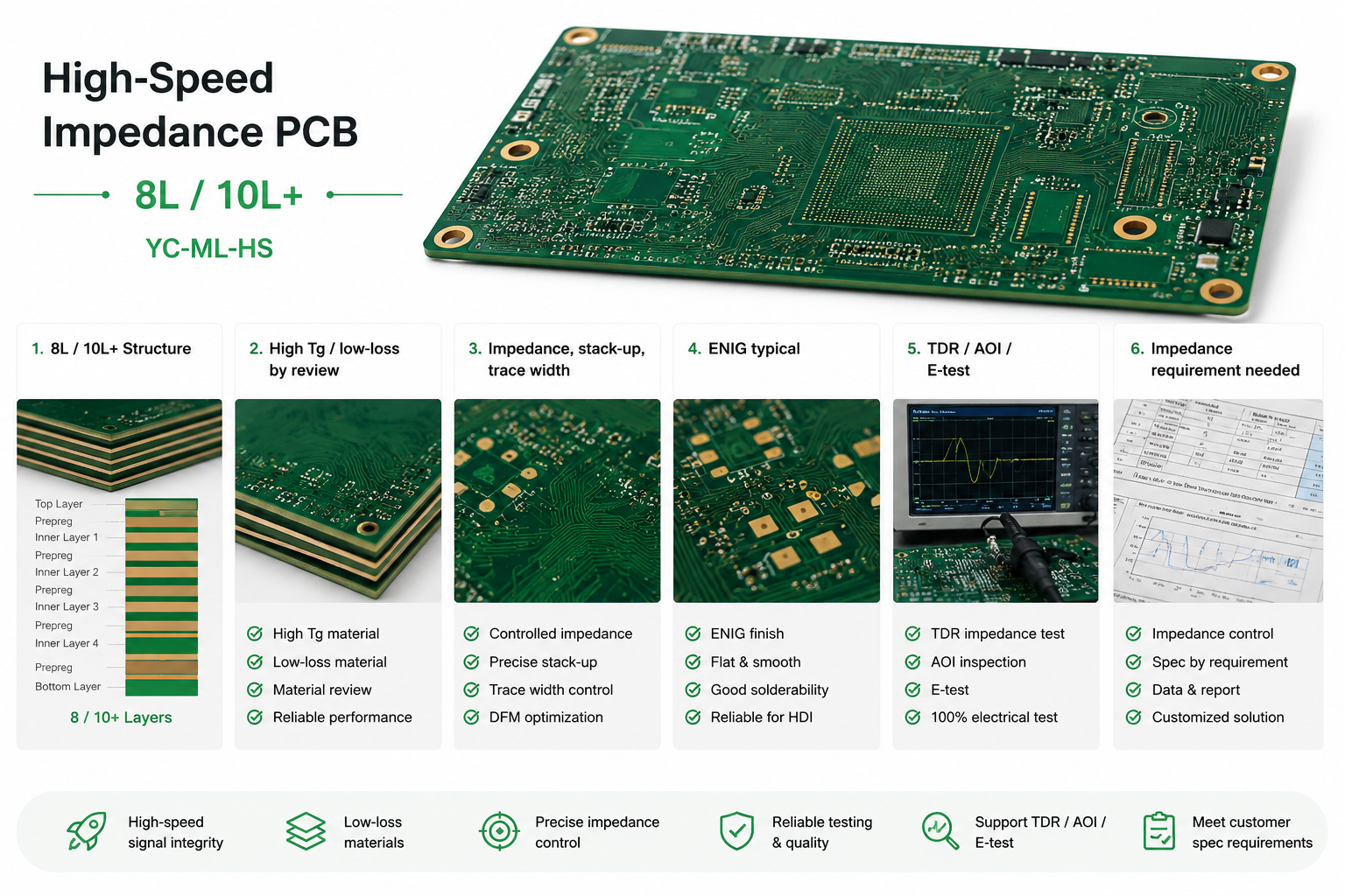
Fine-pitch BGA fan-out can use microvias and controlled trace geometry to route signals within limited board space.
Confirm Before Quotation
Send the following fabrication and assembly information so material, stack-up, HDI structure, testing, price and lead time can be confirmed accurately.
| Parameter | Standard Review Scope | Confirm by File |
|---|---|---|
| Product Route | 20 layer FR4 HDI PCB | Layer function, stack-up and HDI route |
| Finished Thickness | Project-specific 20 layer construction | Stack-up, copper weights, impedance targets and mechanical limits |
| Base Material | FR4 / high Tg FR4 review | Tg, Dk/Df, thermal and reliability needs |
| Layer Count | 20 layer circuit board | Signal / ground / power layer usage |
| HDI Structure | Blind via, buried via, microvia review | Via type, via depth, via-in-pad requirement |
| Routing Density | High density multilayer review | BGA pitch, fan-out and trace spacing |
| Surface Finish | ENIG, OSP, HASL-LF review | Assembly method and storage requirement |
| Impedance | Single-ended and differential review | Stack-up, material, reference plane and trace width |
| Copper Weight | Project-based copper review | Signal, power and thermal areas |
| Testing | AOI, X-Ray, electrical testing support | ICT / FCT if PCBA is needed |
| Assembly Support | SMT, THT and mixed assembly review | BOM, pick-and-place, assembly drawing |
| Files Needed | Gerber, drill, stack-up notes, impedance notes | BOM and test files if PCBA is needed |
20 Layer Stack-Up Example
The layer assignment below is an example rather than a fixed production build. Your final stack-up is calculated from finished thickness, material, copper weight, impedance targets, BGA layout and assembly process.
| Layer | Common Function | Review Focus |
|---|---|---|
| L1 | Signal / SMT | BGA escape, fine pads, ENIG finish |
| L2 | Ground | Return path and shielding reference |
| L3 | Signal | Controlled routing and inner trace review |
| L4 | Power | Power distribution and copper balance |
| L5 | Signal | High density multilayer routing |
| L6 | Ground | Signal reference and EMI support |
| L7 | Signal | Inner routing and via transition |
| L8 | Power | Separated power domain review |
| L9 | Signal | Dense routing or differential pair review |
| L10 | Ground | Center symmetry and reference plane |
| L11 | Ground / Power | Symmetry and plane pairing review |
| L12 | Signal | Controlled route transition |
| L13 | Power | Power integrity and copper balance |
| L14 | Signal | Inner signal layer planning |
| L15 | Ground | Reference plane continuity |
| L16 | Signal | High density routing review |
| L17 | Power | Power plane split review |
| L18 | Signal | Connector and interface routing |
| L19 | Ground | Bottom-side reference support |
| L20 | Signal / Connector | Test access, connector pads, surface finish |
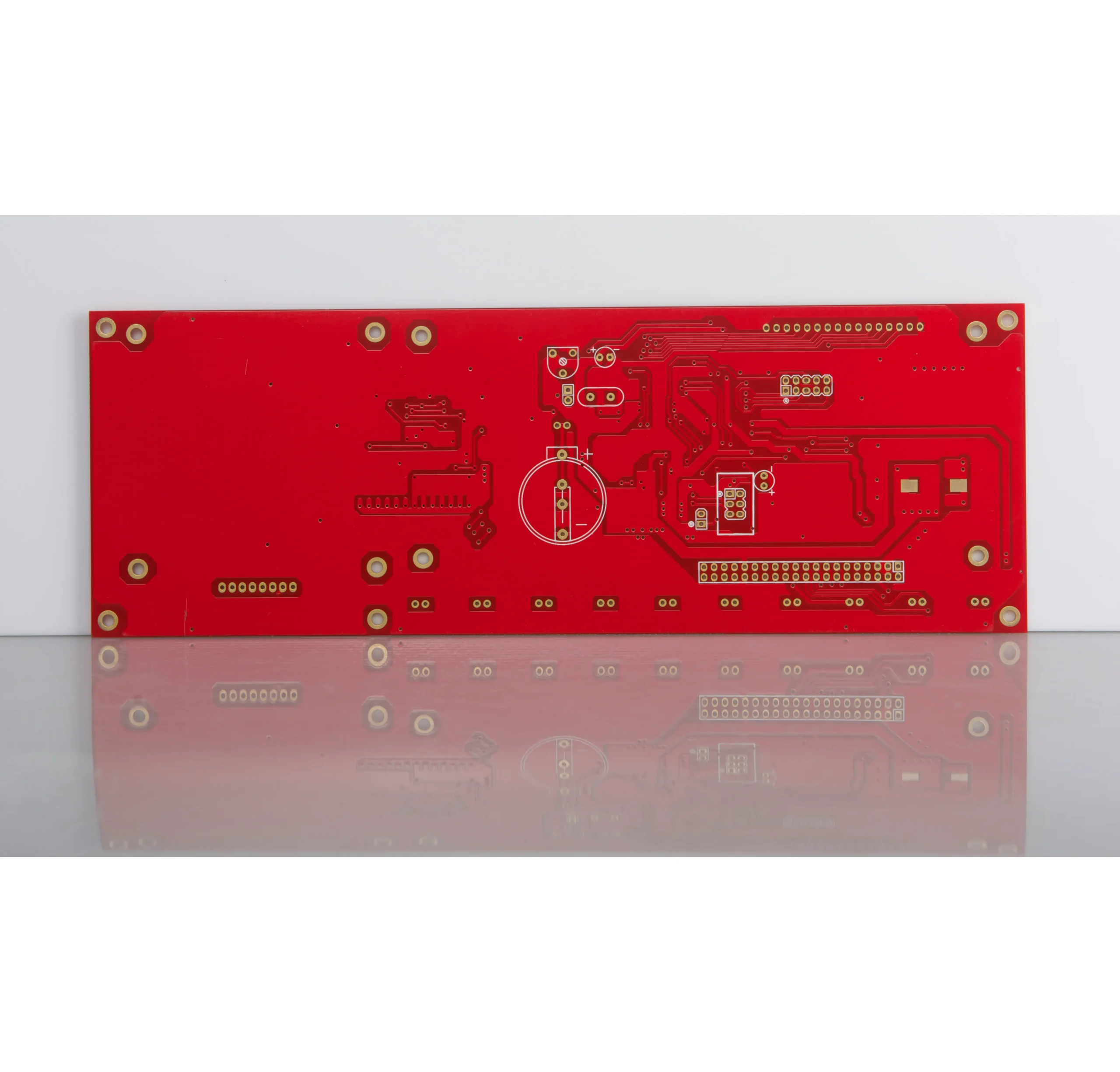
The production stack-up specifies every signal, power and ground layer together with copper and dielectric thicknesses.
HDI Design Checks
Complete stack-up, drill and impedance information reduces engineering queries and helps prevent BGA fan-out, layer registration and assembly issues.
Stack-Up Symmetry
Layer balance, plane pairing and copper distribution are controlled to support the required thickness and reduce warpage risk.
HDI Via Structure
Specify blind vias, buried vias, microvias, via-in-pad and sequential lamination requirements in the drill and stack-up data.
BGA Escape Routing
Provide BGA pitch, pad geometry, fan-out density and reference-layer assignments for manufacturability confirmation.
Impedance Notes
Provide single-ended and differential targets together with reference layers and any required trace geometry.
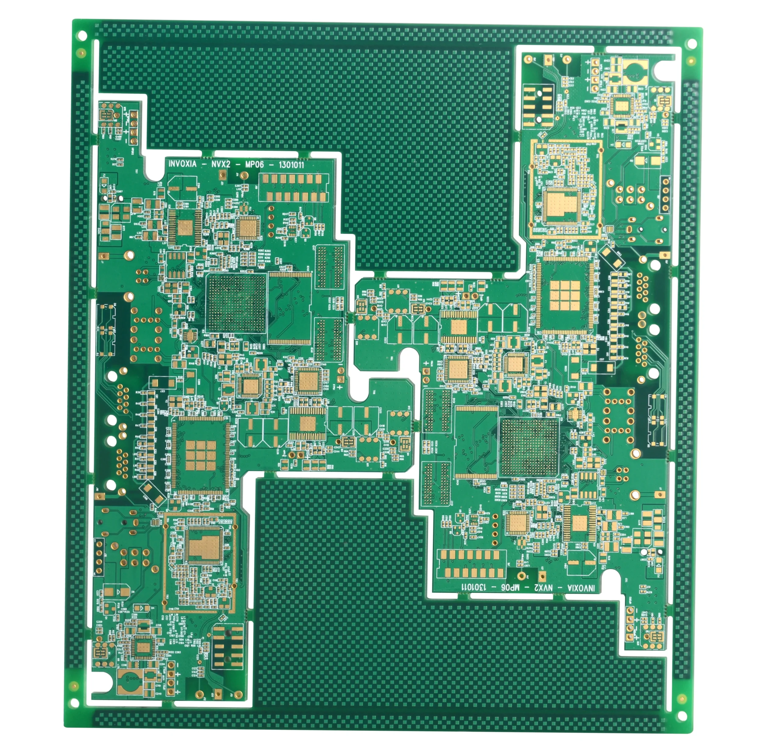
BGA fan-out, microvias, dense traces and reference layers are manufactured from the approved routing and stack-up data.
High Density Multilayer Applications
A 20 layer FR4 HDI PCB is usually selected when lower-layer boards cannot support routing density, signal planning, power domains or compact assembly requirements.

For communication modules, routers, switches and interface boards with multiple signal and connector areas.
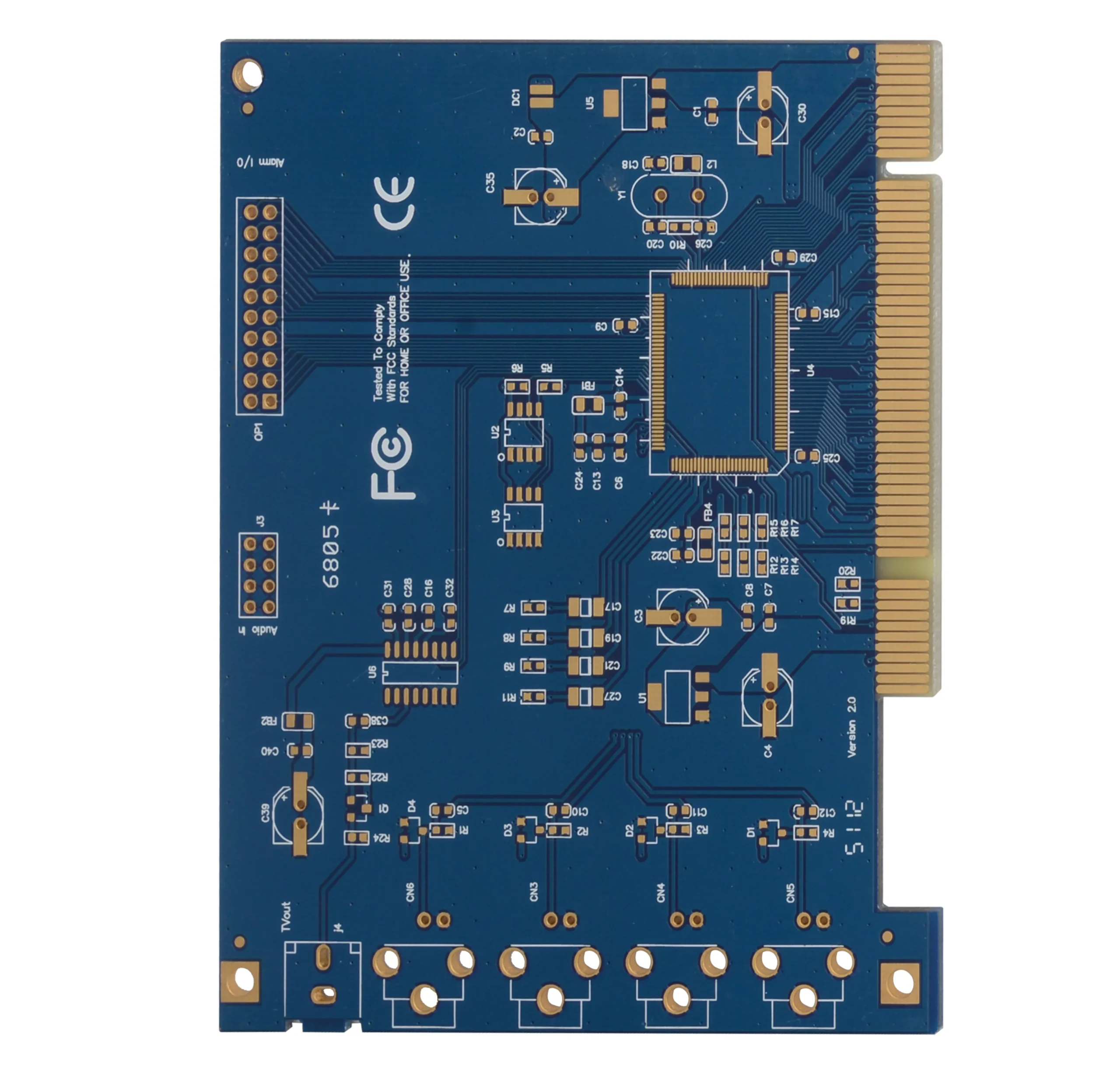
For high density boards that combine processors, memory areas, power domains and high-speed routing.
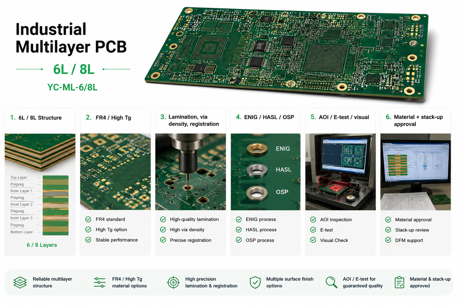
For industrial communication, control and embedded systems where stable layer planning is required.

For compact electronic systems that need dense IC layout, connectors, signal routing and PCBA support.
FR4 Material Selection
FR4, high Tg FR4 and surface finish options can be reviewed for 20 layer HDI and high density multilayer projects. Final material selection should be confirmed according to Tg, Dk/Df, thermal condition, impedance requirement, assembly process and reliability target.
FR4 / High Tg FR4
Reviewed for standard and higher-reliability multilayer PCB projects where FR4 material is suitable for the electrical and thermal requirement.
ENIG / OSP / HASL-LF
Surface finish should be selected according to SMT pad density, storage time, solderability, cost and assembly method.
Impedance Material Notes
If impedance is required, material data and stack-up spacing should be reviewed together before confirming the production route.
20 Layer HDI Manufacturing Flow
A 20 layer FR4 HDI PCB requires tighter process planning than standard lower-layer boards because inner layers, lamination, HDI vias, plating, surface finish and testing all affect production reliability.
Engineering File Review
Gerber, drill, stack-up, impedance notes, HDI via structure and surface finish are checked first.
Inner Layer Imaging and Etching
Inner circuits are formed layer by layer according to the approved production files.
Lamination and HDI Via Process
FR4 cores, prepreg, copper layers and HDI via structures are processed according to the confirmed route.
Drilling and Copper Plating
Plated connections, microvia paths and through-hole structures are controlled during drilling and plating.
Outer Layer, Solder Mask and Finish
Outer pattern, solder mask, silkscreen and surface finish are completed before inspection.
Inspection, Testing and Packing
AOI, X-Ray, electrical testing and final inspection are arranged according to project requirements.

CAM engineering verifies layer data, drill files, stack-up, impedance requirements and panelization before production.
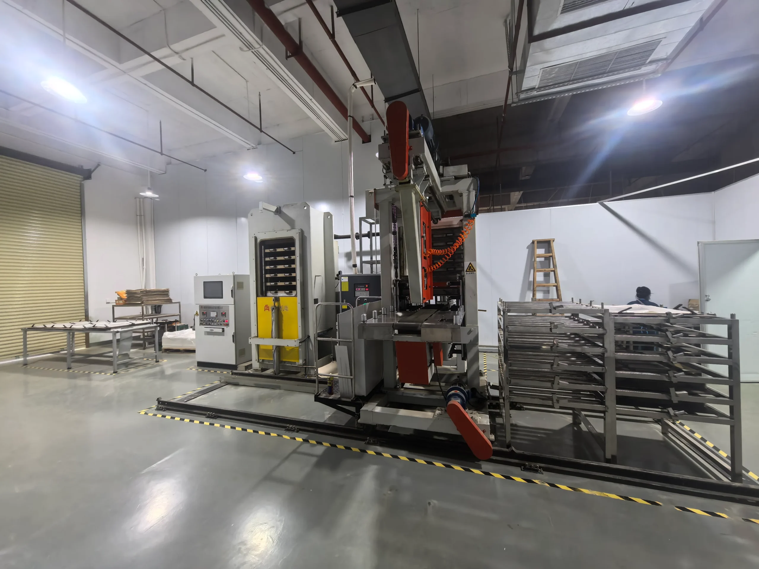
Layer alignment, resin flow and stack-up balance are key points for high-layer HDI boards.
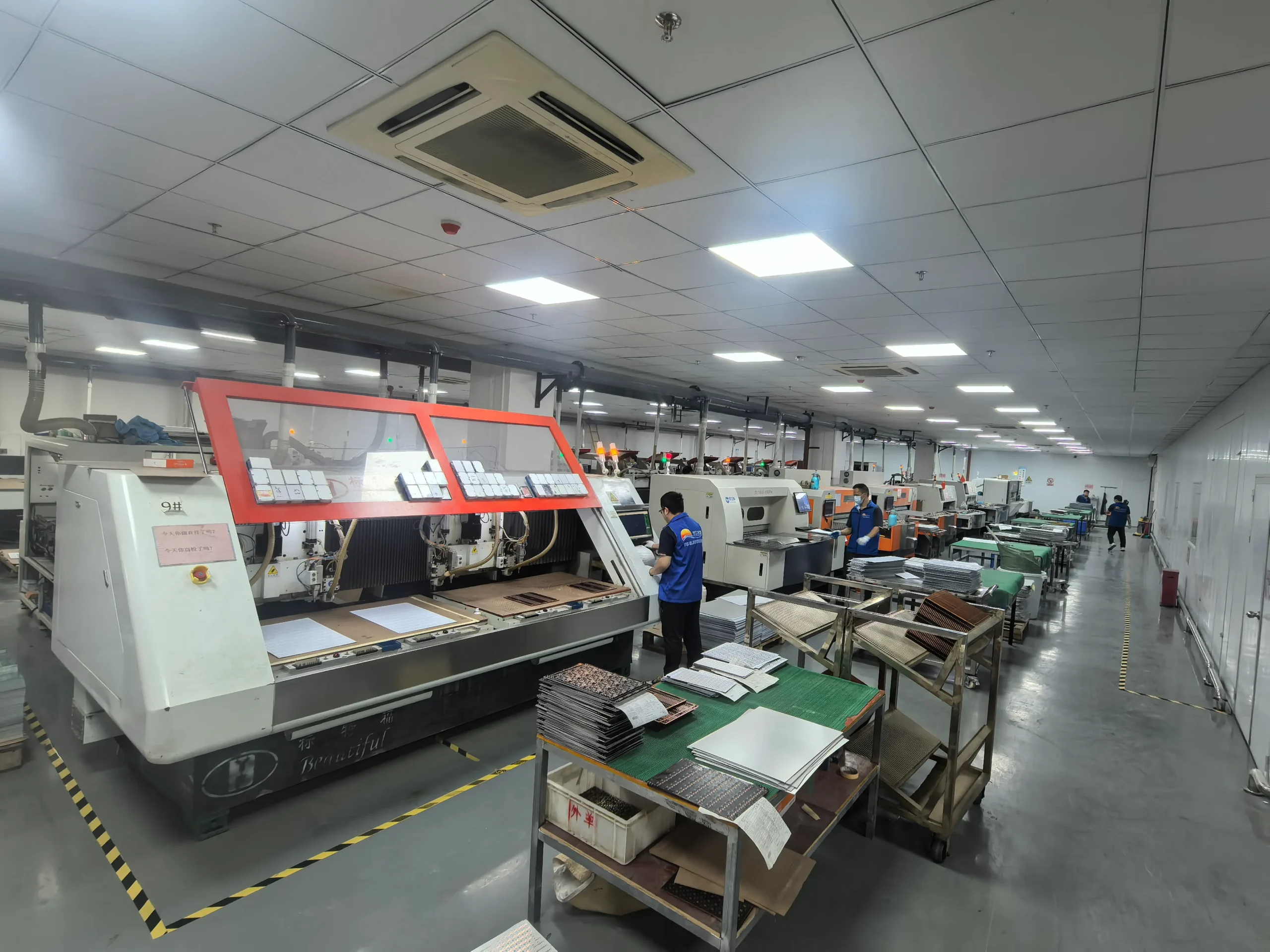
Microvia, via-in-pad and BGA breakout requirements are controlled through the specified drilling, filling and plating process.
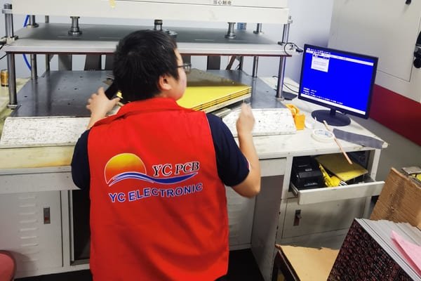
AOI, X-Ray and electrical tests help reduce open, short and internal connection risk.
Quality Checks Before Shipment
For advanced HDI board orders, quality checks focus on inner layer accuracy, layer registration, lamination reliability, plated connections, dense BGA areas, surface finish, electrical testing and optional PCBA test route.
Layer Registration Risk
Layer alignment and copper distribution are reviewed to reduce high-layer stack-up risk before production release.
HDI Via Reliability
Blind vias, buried vias, microvias and plating routes are reviewed according to the submitted HDI structure.
BGA and X-Ray Review
Dense BGA areas, via-in-pad or hidden solder joints can require X-Ray or assembly process review.
AOI Inspection
Checks circuit pattern defects, open trace risk, short risk, missing pads, over-etching and under-etching.
Impedance Review
Impedance notes, reference layers, trace widths and differential pairs are reviewed according to the submitted stack-up.
Final Release
Packing, quantity, labels, shipment method and delivery requirement are checked before release.
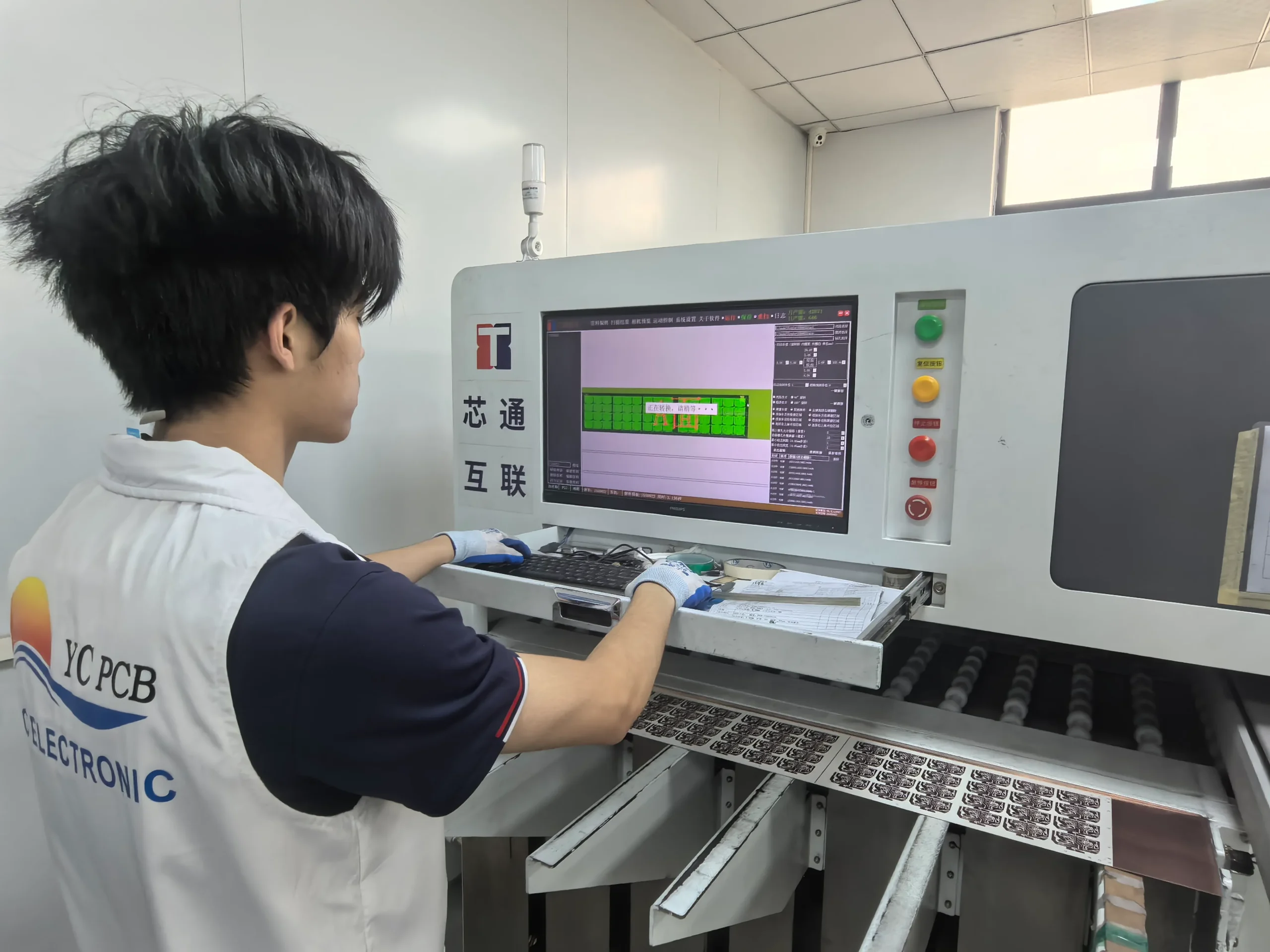
AOI, X-Ray and electrical testing verify inner-layer patterns, plated interconnections and finished-board continuity.

Dense routing, BGA pads and fine interconnect areas are checked for pattern accuracy, pad quality and electrical continuity.
PCB Assembly Support
YC PCB supplies bare 20 layer HDI boards and complete PCBA services. For assembly orders, provide the BOM, pick-and-place file, assembly drawings, programming data and acceptance test requirements.
SMT Assembly
For ICs, fine-pitch components, resistors, capacitors and compact electronics.
THT Assembly
For connectors, terminal parts, pin headers and mechanical interface components.
Testing Review
ICT, FCT, programming and custom functional testing are available when procedures and fixture requirements are supplied.
Component Sourcing
Components can be sourced from the approved BOM, with alternates confirmed before purchasing when necessary.
20 Layer HDI Route Comparison
A 20 layer HDI build is most suitable when routing density, BGA pitch, power-plane planning or board-size constraints cannot be met with a simpler multilayer structure.
| PCB Route | Better For | Buyer Decision |
|---|---|---|
| 16 Layer FR4 PCB | High-layer projects with lower routing density | Choose when 16 layers can support routing, power and signal needs. |
| 20 Layer FR4 HDI PCB | Dense BGA, advanced routing and multi-reference-plane projects | Choose when lower-layer routes cannot handle density or layer planning. |
| Standard Multilayer PCB | Projects without blind / buried via needs | Use when through-hole vias and normal stack-up can support the design. |
| High-Frequency PCB | RF or signal-sensitive applications beyond normal FR4 limits | Review when Dk/Df, loss and frequency become key concerns. |
| PCBA Route | Complete electronic module manufacturing | Use when PCB fabrication, assembly, sourcing and testing should be combined. |
Common 20 Layer HDI Projects
Quotation, lead time and testing are determined by the Gerber data, stack-up, HDI structure, material availability, quantity and assembly scope.
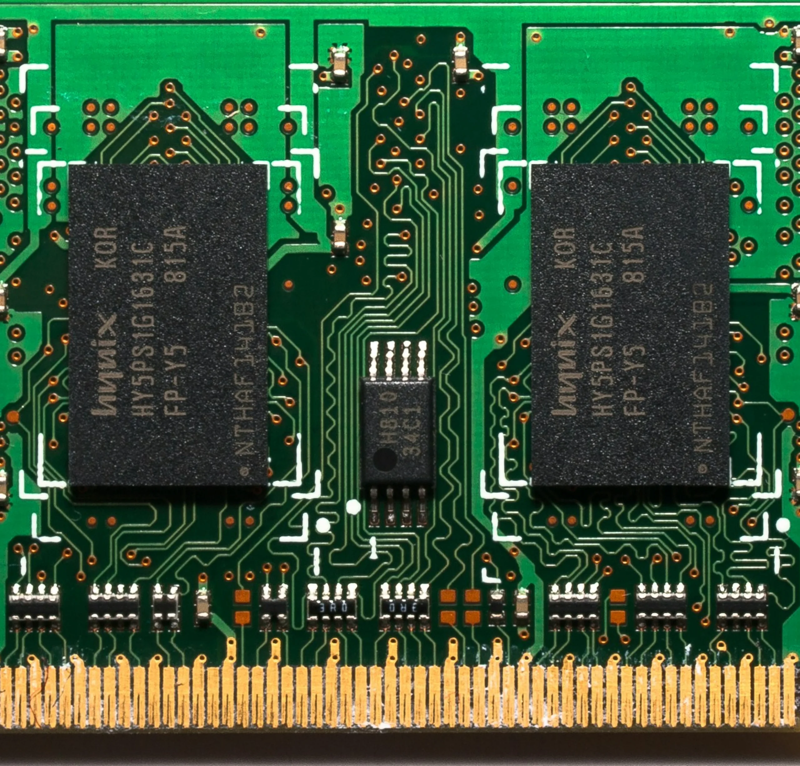
Common requirements include controlled impedance, dense BGA fan-out, connector interfaces and full electrical testing.
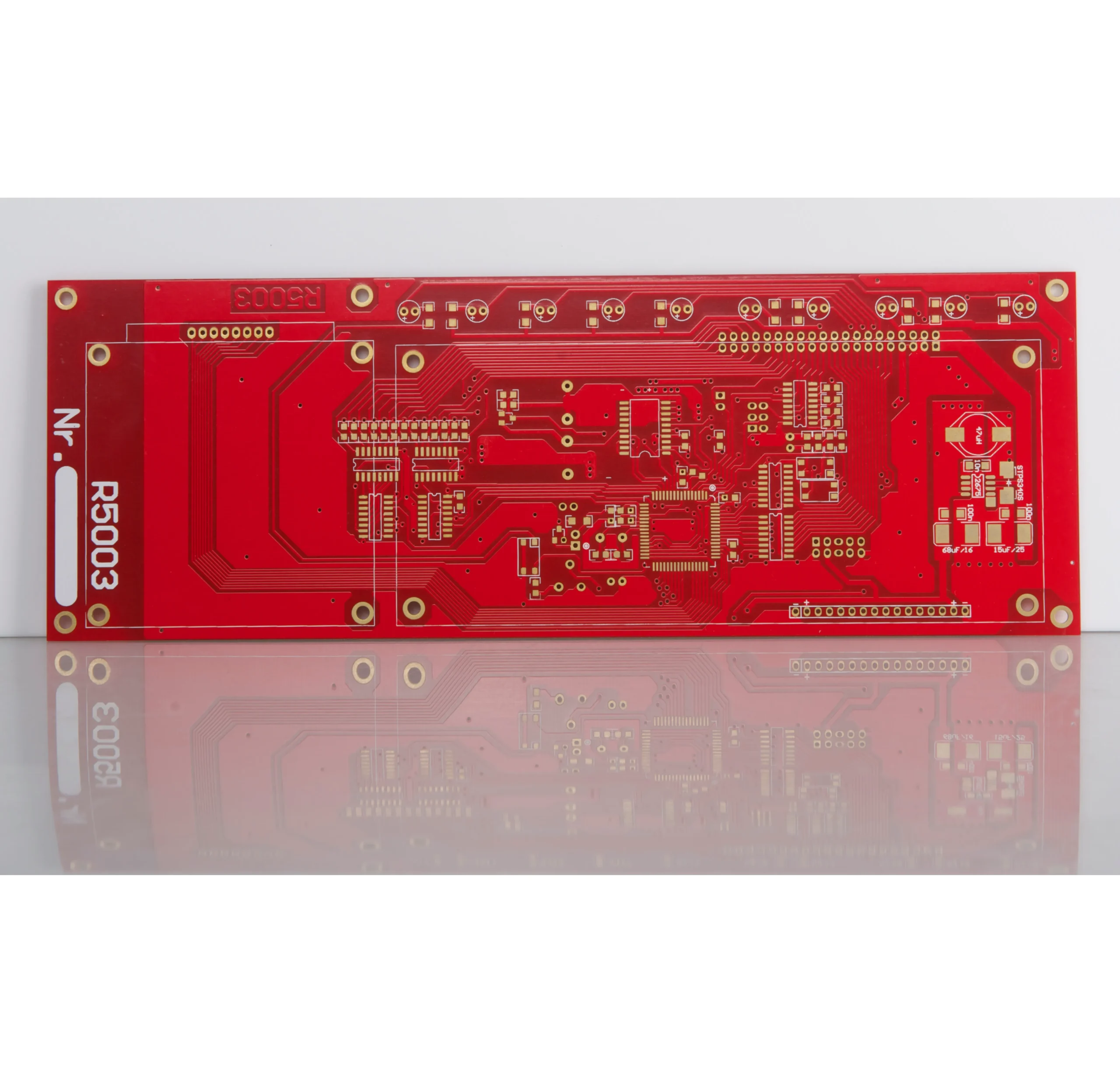
Server boards may require multiple power domains, dense IC placement, continuous reference planes and complete PCBA testing.
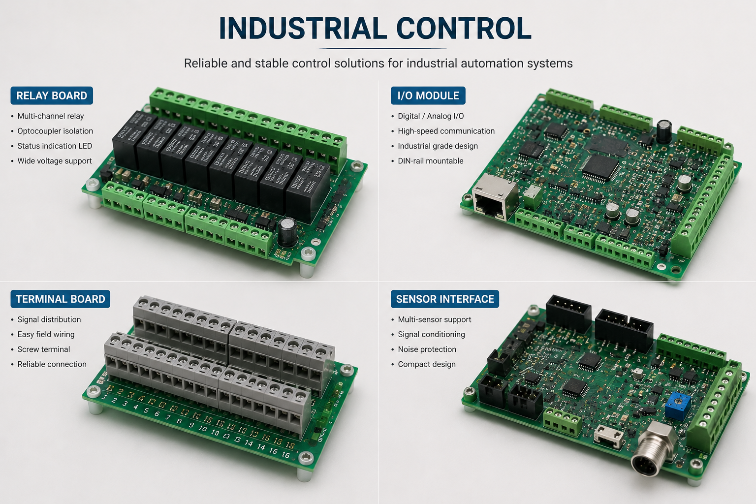
Industrial builds can include environmental requirements, reinforced connectors, defined test points and functional acceptance testing.
Files Needed for Quotation
Complete RFQ files allow YC PCB to confirm the stack-up, HDI structure, impedance, testing scope, unit price and production lead time accurately.
- Gerber files
- Excellon drill file
- Stack-up notes
- Board thickness
- Copper weight
- HDI via notes
- Impedance notes
- Surface finish
- Quantity
- Target lead time
- BOM for PCBA
- Testing requirement
20 Layer FR4 HDI PCB FAQ
Common procurement and engineering questions for HDI PCB 20 layer, 20 layer FR4 HDI, high density multilayer and advanced HDI board projects.
What is a 20 layer FR4 HDI PCB?
It is a high density multilayer PCB using FR4 material and HDI interconnects such as blind vias, buried vias, microvias and via-in-pad. It is selected when a standard multilayer structure cannot provide enough routing density, BGA fan-out or reference-plane capacity.
When should I choose HDI PCB 20 layer instead of a lower-layer PCB?
Choose this construction when the design requires additional signal layers, multiple reference planes, compact BGA escape routing, dense interconnections or more power and ground distribution than a lower-layer board can provide.
Can FR4 be used for high density multilayer PCB projects?
Yes. FR4 and high Tg FR4 are suitable for many high density multilayer boards. The selected laminate must meet the required Tg, Dk/Df, thermal conditions, stack-up and reliability targets.
What files are needed for 20 layer HDI stack-up review?
Please send Gerber files, Excellon drill file, stack-up notes, board thickness, copper weight, impedance notes, surface finish requirement and quantity. If PCBA is needed, send BOM, pick-and-place file, assembly drawing and test requirements.
Can YC PCB review blind vias and buried vias?
Yes. YC PCB supports blind vias, buried vias, microvias and via-in-pad constructions based on the drill data, layer structure, aspect ratio and sequential lamination requirements.
Does a 20 layer circuit board always need HDI?
Not always. Some 20 layer boards use conventional plated through holes. HDI is typically required for fine-pitch BGA fan-out, very dense routing, limited board space or advanced interconnect requirements.
Can YC PCB support impedance review for 20 layer FR4 HDI?
Yes. Submit the impedance table, reference layers and target values. The final trace geometry is calculated from the selected laminate, copper thickness and dielectric spacing.
Can this product route support PCBA?
Yes. YC PCB provides SMT, THT and mixed assembly for 20 layer FR4 HDI projects. Submit the BOM, placement file, assembly drawings, programming files and test requirements with the PCB data.
What is the difference between advanced HDI board and standard multilayer PCB?
An advanced HDI board uses high density interconnect features such as microvias, blind vias, buried vias, via-in-pad or dense BGA fan-out. A standard multilayer PCB may use normal through-hole vias and lower routing density.
How do you check quality before shipment?
Quality control can include CAM verification, inner-layer AOI, drilling and plating checks, X-Ray inspection, electrical testing, final inspection and controlled packing according to the order requirements.
Is ENIG required for 20 layer FR4 HDI PCB?
ENIG is commonly selected for dense SMT pads, fine-pitch components and longer storage. OSP or lead-free HASL may also be suitable depending on pad geometry, assembly method, shelf-life and cost target.
Can YC PCB support prototype and small batch 20 layer HDI orders?
YC PCB supports prototypes, small batches and volume production. Minimum order conditions depend on the laminate, HDI construction, panel utilization and assembly scope.
How is the lead time confirmed?
Lead time depends on stack-up, HDI structure, material availability, surface finish, testing requirement, quantity and whether PCBA is included. Send complete files for a practical quotation and schedule review.
What makes 20 layer FR4 HDI difficult to manufacture?
Key challenges include layer registration, lamination stability, via reliability, resin flow, copper balance, BGA escape density, impedance consistency and final electrical testing.
Should I choose 20 layer FR4 HDI or 16 layer PCB?
If routing density, signal layer count, BGA fan-out or power plane planning can be handled with 16 layers, a 16 layer route may be more cost-effective. Choose 20 layer FR4 HDI when the design needs more routing and reference-layer freedom.
Can I send only Gerber files for initial review?
Yes. Gerber and drill files are sufficient for an initial feasibility check. Stack-up, impedance, BOM and testing information are still required to finalize the price, lead time and production process.
Send Your PCB Files
Send Gerber, drill files, stack-up, HDI via details, impedance targets, copper weights, surface finish, quantity and PCBA files. YC PCB will confirm feasibility, pricing and production lead time.
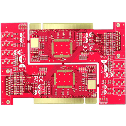
Quotations are based on the approved stack-up, HDI structure, material, testing scope and order quantity.
Send Your 20 Layer HDI PCB Requirements
Tell us what you need. For Gerber files, drill data, stack-up, HDI via notes, impedance tables, BOM or other attachments, email them directly to sales@ycelectronic.com after submitting this form.
 English
  Japanese
  French
  German
  Spanish
  Italian
  Portuguese
  Russian
  Dutch
Dutch  Turkish