 Skip to content
Double Sided FR4 PCB 3-5 Day Prototype Delivery.
YC PCB manufactures custom 2-layer FR4 printed circuit boards from Gerber files for industrial control, LED driver modules, golden finger connector boards, communication electronics, power boards, and assembled PCBA projects.
Supported surface finishes include OSP, HASL, lead-free HASL, and ENIG. Solder mask options include standard colors and high-reflectance white or green for LED applications. Board forming includes CNC milling, V-Cut routing, tab routing, and custom mould operations. Optional end-to-end PCBA integration is available for BOM sourcing, SMT, DIP, functional testing, and final packing.




Double Sided FR4 PCB Product Options
Select by application, solder mask, via requirement, surface finish, golden finger design, forming method, and PCBA requirement. Each item can be quoted from Gerber files, drawings, BOM, or reference samples.
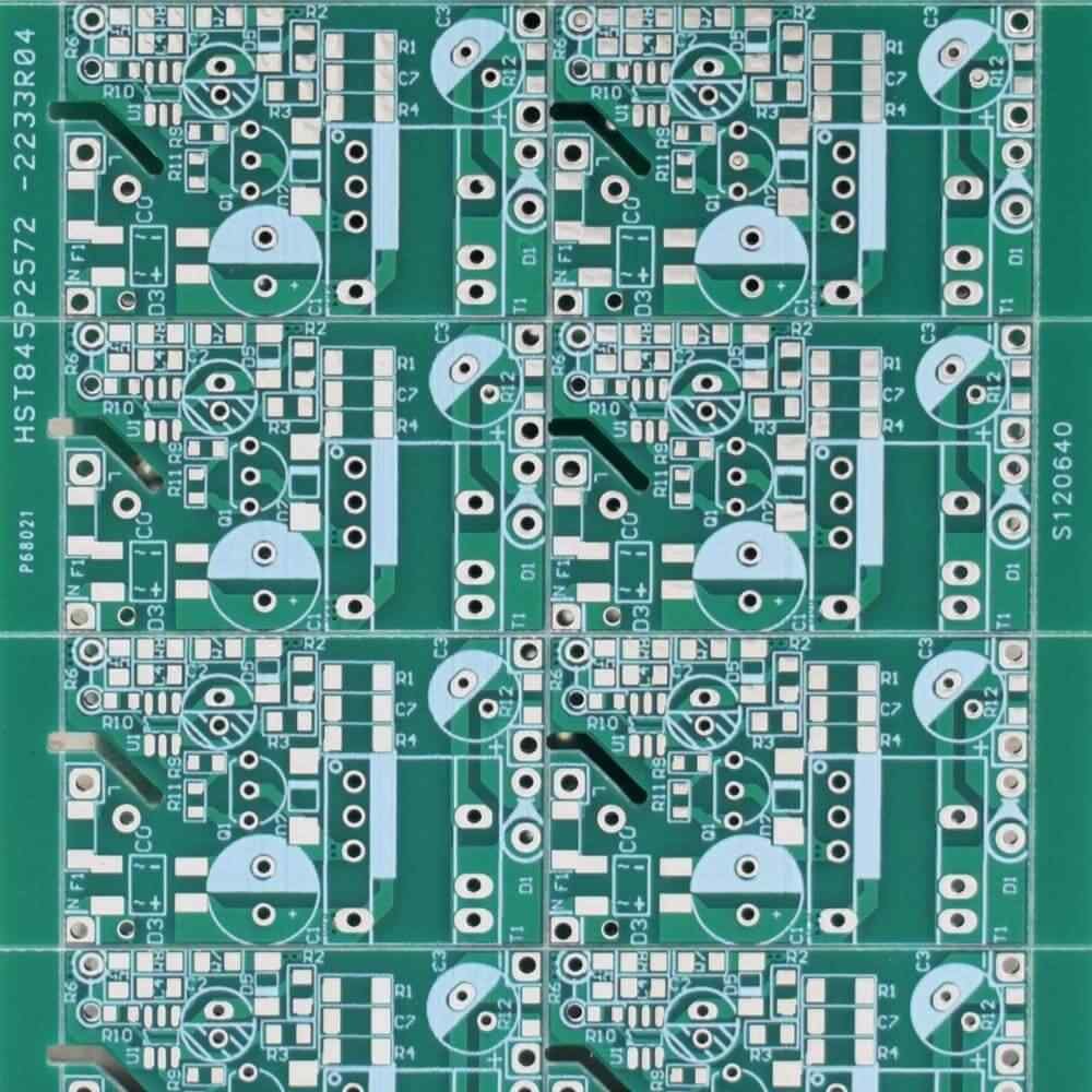
Standard Double Sided FR4 PCB
General 2-layer FR4 PCB with plated through-hole vias for control boards, sensor boards, interface modules, power boards, and consumer electronics.
- • Gerber and drill file completeness review
- • Annular ring, PTH via, and finished hole tolerance check
- • Copper clearance and solder mask bridge evaluation
- • Panelization method: individual, V-Cut, or tab routing
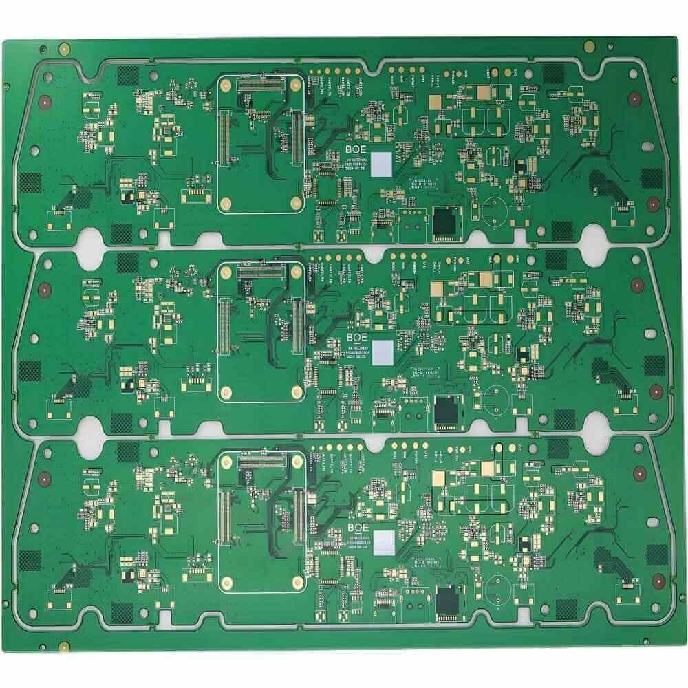
Industrial Control Double Layer FR4 PCB
2-layer FR4 PCB for relay control, IO modules, sensor interfaces, machine control boards, terminal boards, and switching control circuits.
- • High-current trace routing and copper clearance validation
- • Terminal pad design for insertion force and soldering reliability
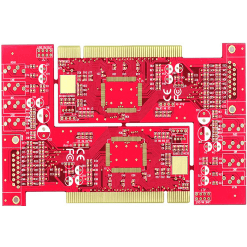
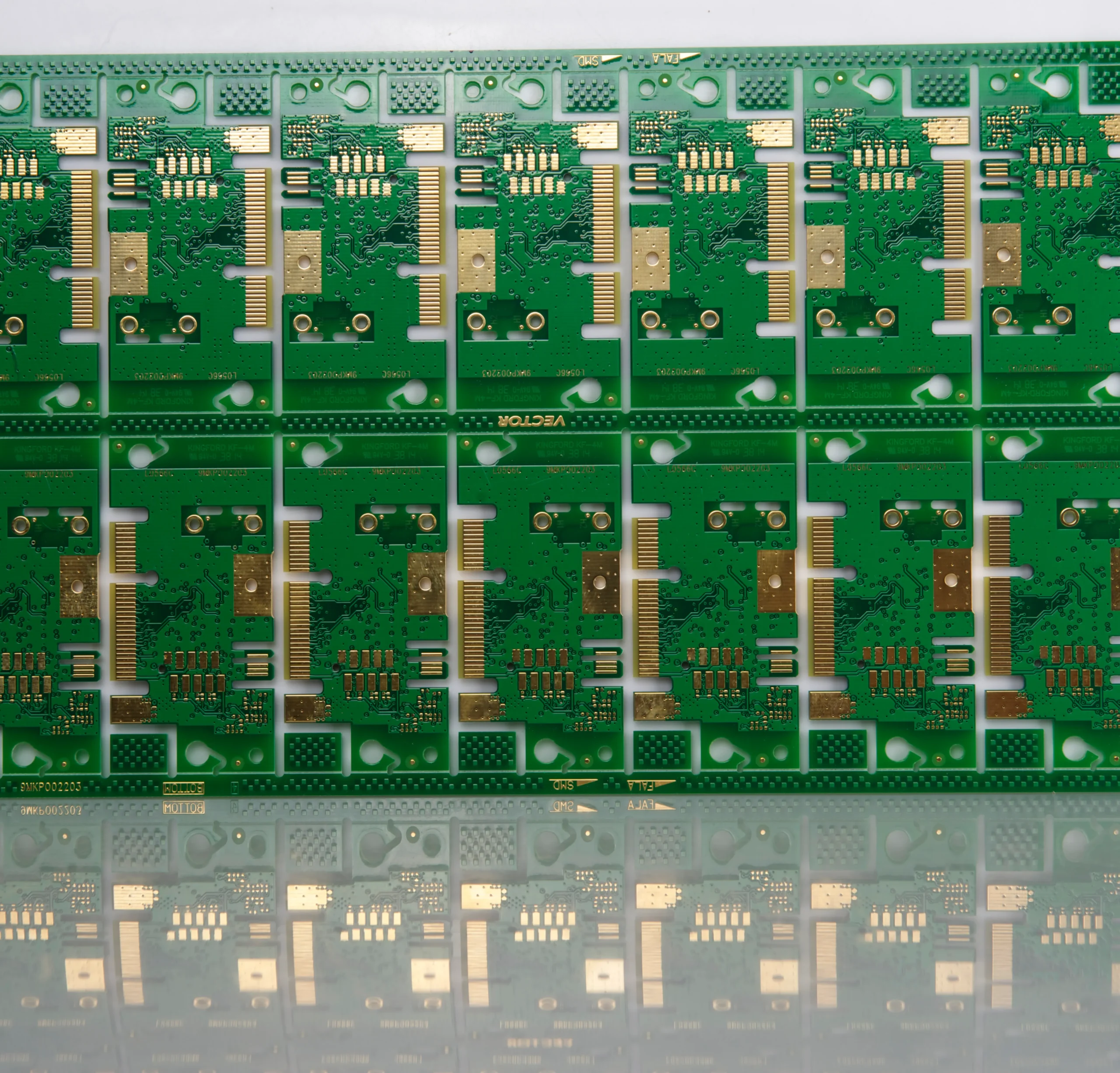
Golden Finger Double Layer FR4 PCB
2-layer FR4 PCB with golden finger edge connector for plug-in modules, control cards, communication boards, and connector interface boards.
- • Edge bevel angle verification
- • Finger pitch and connector tolerance review
- • Gold plating thickness validation based on connector use requirements
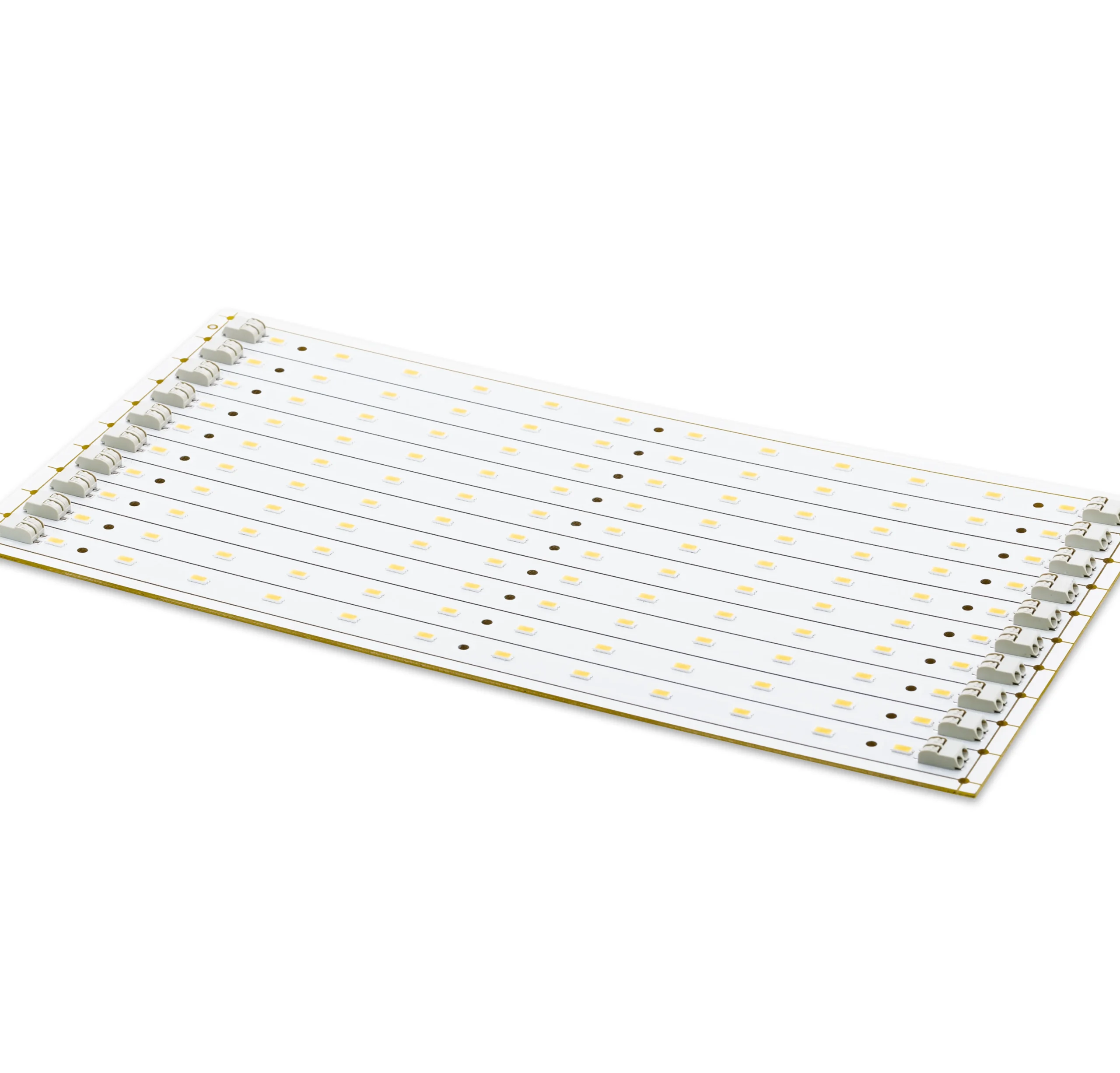
Double Sided LED FR4 PCB
Double sided FR4 PCB for LED control circuits, LED driver modules, lighting interfaces, and mixed LED electronic assemblies.
- • High-reflectance solder mask for LED photometric performance
- • LED polarity and solder pad verification
- • Thermal copper area and current path review
Communication Electronics FR4 PCB
Double sided FR4 PCB for communication interface boards, signal modules, adapter boards, and low-to-medium complexity electronic products.
- • Routing density assessment for 2-layer versus 4-layer conversion
- • Surface finish selection for SMT pad reliability and storage stability

Double Sided FR4 PCB Assembly
Double sided PCB fabrication plus component sourcing, SMT, DIP, functional testing, and packing for finished electronic boards.
- • BOM validation and component sourcing feasibility
- • SMT / DIP process sequence review
- • Functional testing and packing method confirmation
Double Sided FR4 PCB Image Gallery
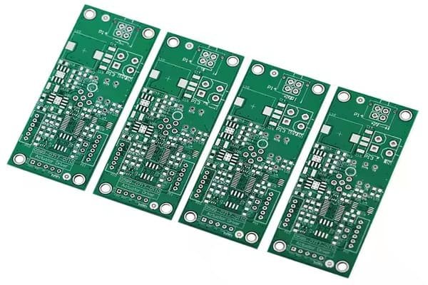
Standard 2-Layer FR4 PCB
Green solder mask, PTH vias, HASL / OSP / ENIG options.
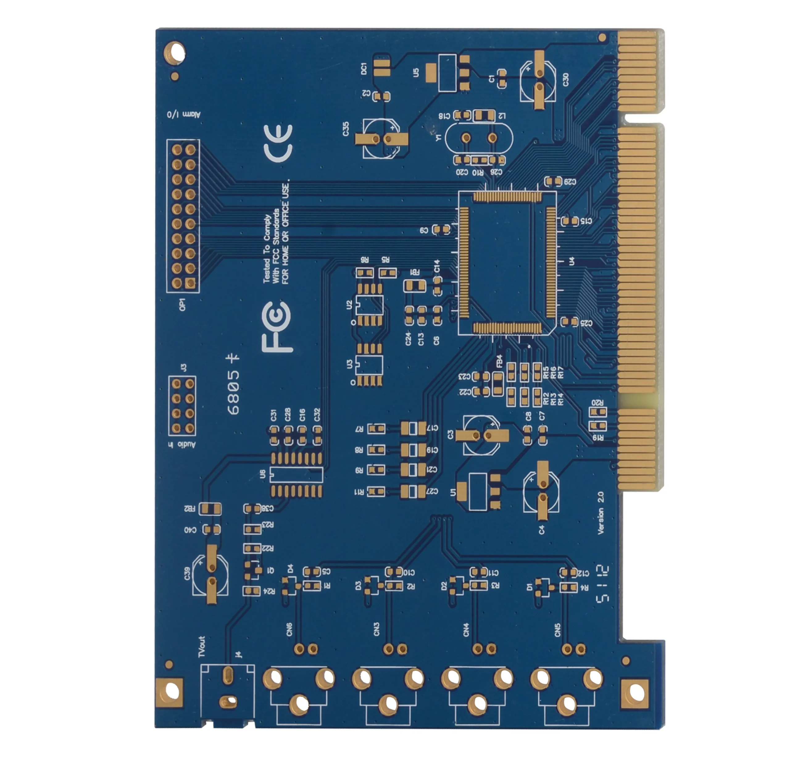
Golden Finger FR4 PCB
Edge connector board with ENIG or gold finger process.

White LED FR4 PCB
High-reflectance solder mask for LED control and lighting modules.

Double Sided FR4 PCBA
PCB fabrication plus SMT, DIP, functional testing, and packing.
Compare Double Sided FR4 PCB Parameters
This table is designed for engineering buyers. It shows product type, material, via structure, solder mask, finish, forming method, lead time, MOQ, and quote entry in one view.
| Image | Product / Part No. | Base / Type | Layer | Via / Hole | Copper | Trace / Space | Solder Mask | Surface Finish | Forming | Lead Time | MOQ | Typical Application | Quote |
|---|---|---|---|---|---|---|---|---|---|---|---|---|---|
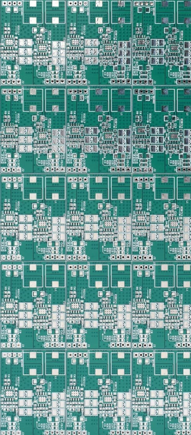 | Standard Double Sided FR4 PCB YC-DF4-001 General 2-layer PCB | Double layer FR4 | 2L | PTH / 0.30mm mechanical drill reference | 1-3oz | 0.15mm trace / 0.15mm space standard; finer geometries reviewed per design complexity | Green / Blue / Black / Red | OSP, HASL, ENIG | CNC Milling + V-Cut / Mould | 3-5 working days | 1 pcs | Control boards, modules, consumer electronics | |
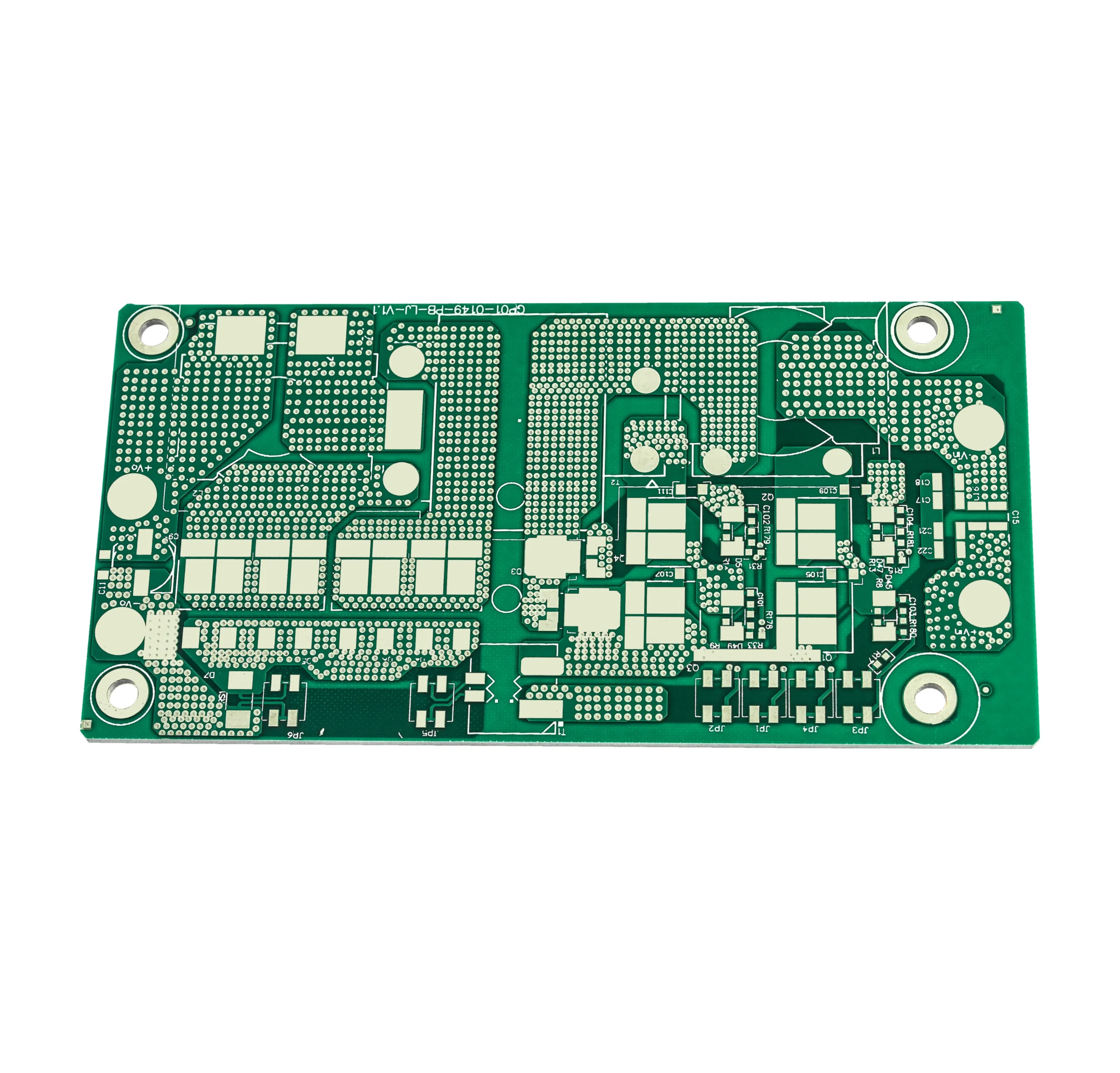 | Industrial Control Double Layer FR4 PCB YC-DF4-IC Industrial control series | Double layer FR4 | 2L | PTH / terminal holes | 1-3oz | Per Gerber and engineering review | Green / Custom | OSP, HASL, ENIG | CNC Milling + V-Cut / Mould | 3-5 working days | 1 pcs | Relay boards, IO modules, industrial control | |
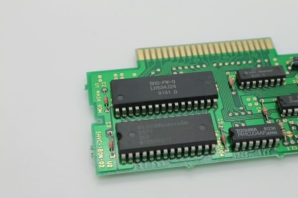 | Golden Finger Double Layer FR4 PCB YC-DF4-GF Edge connector PCB | Double layer FR4 / Golden finger | 2L | PTH / edge connector design | 1-2oz | Per connector pitch and engineering review | Green / Black | ENIG / gold finger process | CNC Milling / Edge bevel | 3-5 working days | 1 pcs | Plug-in modules, interface boards, control cards | |
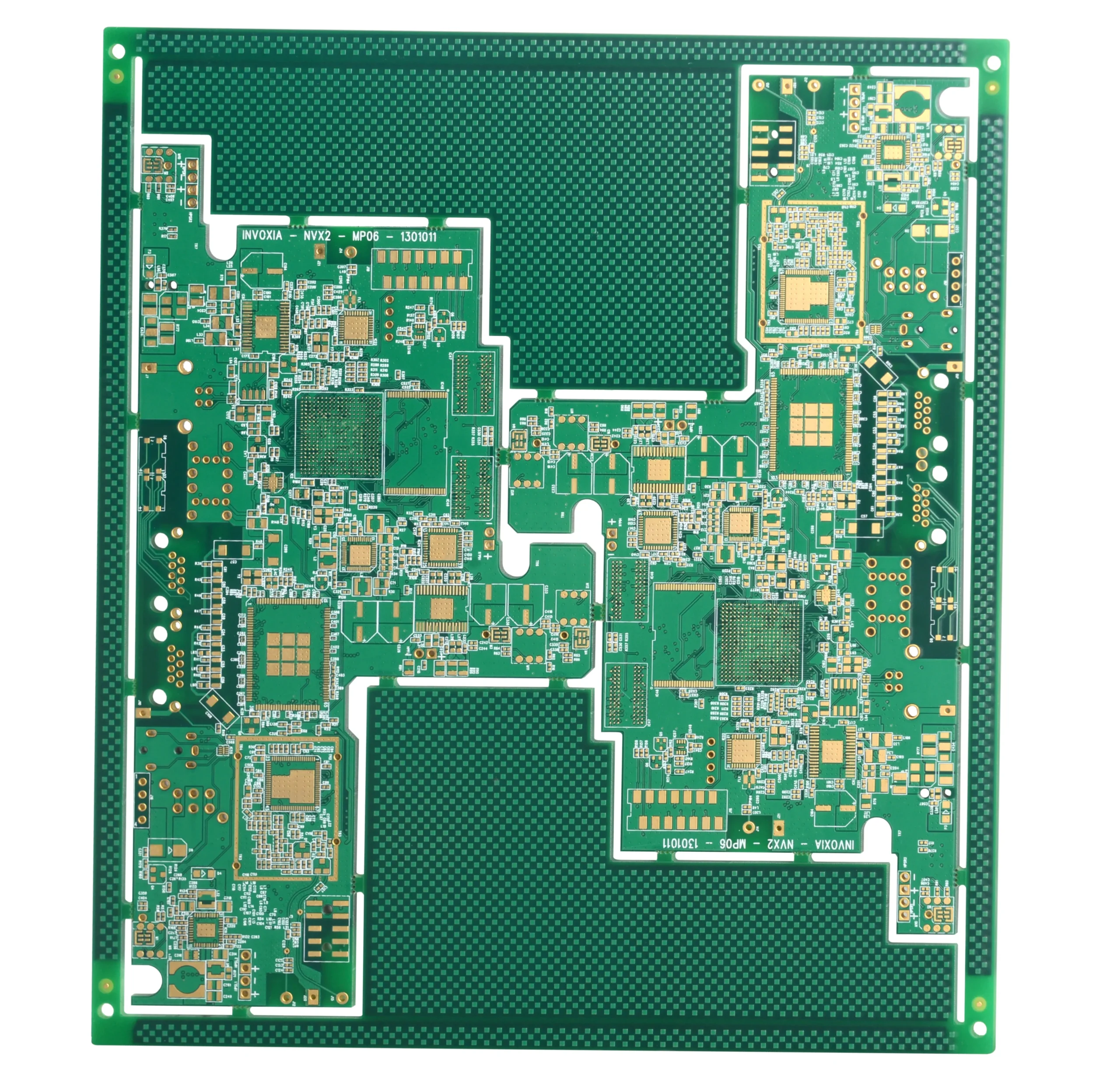 | Double Sided LED FR4 PCB YC-DF4-LED LED control / LED driver board | Double layer FR4 | 2L | PTH | 1-2oz | 0.15mm trace / 0.15mm space standard; finer geometries reviewed per design complexity | High-reflectance white / silver ink | OSP, HASL, ENIG | CNC Milling + V-Cut / Mould | 3-5 working days | 1 pcs | LED driver, lighting control, LED module | |
 | Communication Electronics FR4 PCB YC-DF4-COM Communication interface board | Double layer FR4 / 4L option | 2L / 4L review | PTH / signal via | 1oz typical | Per Gerber and engineering review | Green / Black | OSP / ENIG | CNC Milling / Panel | 3-5 working days | 1 pcs | Interface board, signal module, adapter board | |
 | Double Sided FR4 PCB Assembly YC-DF4-PCBA PCB + BOM + Assembly + Test | FR4 PCB / PCBA | 2L | Per Gerber and engineering review | Per Gerber and engineering review | Per Gerber and engineering review | Custom | OSP, HASL, ENIG | Panel / Finished board | By BOM + quantity | 1 pcs | Finished control boards, LED PCBA, sensor PCBA |
Final capability depends on board thickness, copper weight, drill density, via structure, solder mask bridge, surface finish, and panel design.
Process Limit Notes for Double Sided FR4 PCB
Double sided FR4 PCB uses plated through holes to connect top and bottom copper layers. Drill size, annular ring, copper plating, and via clearance are reviewed during DFM preparation.
0.15 / 0.15mm is the standard reference for stable production. Smaller values or dense routing should be reviewed based on copper weight, solder mask bridge, and etching compensation.
Golden finger boards require additional review of bevel angle, edge connector tolerance, pad pitch, surface finish, and insertion durability requirements.
2-Layer FR4 PCB Design Capability Reference
The following values are reference ranges for quotation screening. Final manufacturability depends on copper weight, board thickness, via density, solder mask bridge, hole tolerance, and surface finish.
| Parameter | Standard Capability | Advanced / Review Required | Engineering Note |
|---|---|---|---|
| Min Trace / Space | 0.15 / 0.15 mm | Below 0.15 mm by review | Affected by copper weight and etching compensation. |
| Mechanical Drill | 0.30 mm reference | Smaller holes by review | Finished hole tolerance and plating reliability must be checked. |
| Board Thickness | 0.6 - 2.4 mm common range | 0.4 - 3.2 mm by review | Thin and thick boards require additional process confirmation. |
| Copper Weight | 1oz standard | 2oz / 3oz by design review | Heavy copper affects trace spacing and etching tolerance. |
| Surface Finish | HASL / OSP | ENIG / golden finger | ENIG is preferred for flat SMT pads or connector applications. |
| Panelization | Individual / V-Cut / tab routing | Custom mould forming by review | Panel design affects SMT efficiency, yield, and shipment safety. |
2-Layer FR4 PCB Production from Gerber and Drill Files.
Double sided FR4 production requires controlled laminate selection, accurate drilling, reliable through-hole plating, top-bottom registration, solder mask alignment, surface finish stability, electrical net testing, and final visual inspection.
YC PCB supports standard double sided FR4 PCB, industrial control boards, golden finger boards, LED FR4 control boards, communication interface boards, and double sided PCBA production.
General Capability Range
Thickness selection depends on copper weight, via diameter, finished hole tolerance, and mechanical strength requirements. Consult engineering for specifications below 0.6mm or above 2.4mm.
Prototype and Batch Delivery Timeline
Lead time is confirmed after Gerber review, material availability check, surface finish confirmation, and payment release. Prototype delivery and batch production are managed through separate scheduling workflows.
Prototype Delivery
For approved 2-layer FR4 designs using standard materials and available production capacity.
Batch Production
Typical range after file approval, payment release, and confirmed production route.

Recent Shipping Record
Production Images for Double Sided FR4 PCB
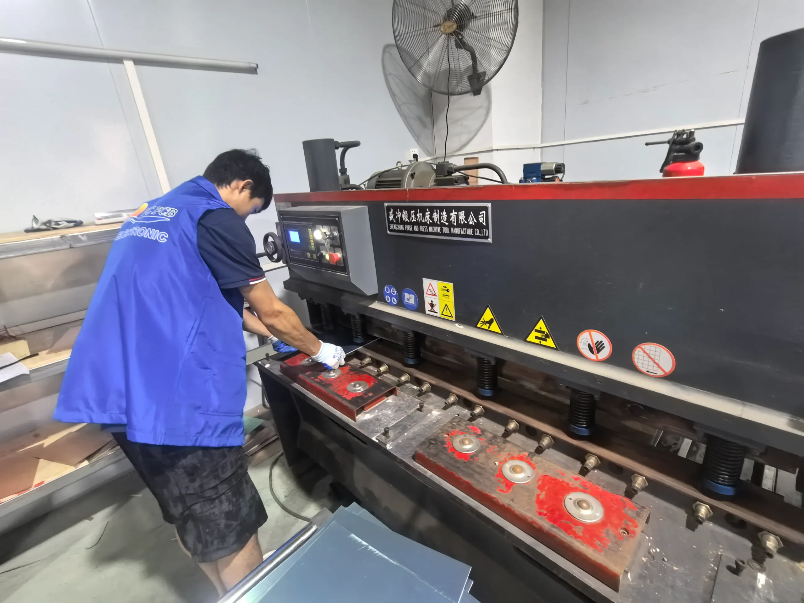
PCB Production Line
Real factory photo of drilling, or routing workshop.
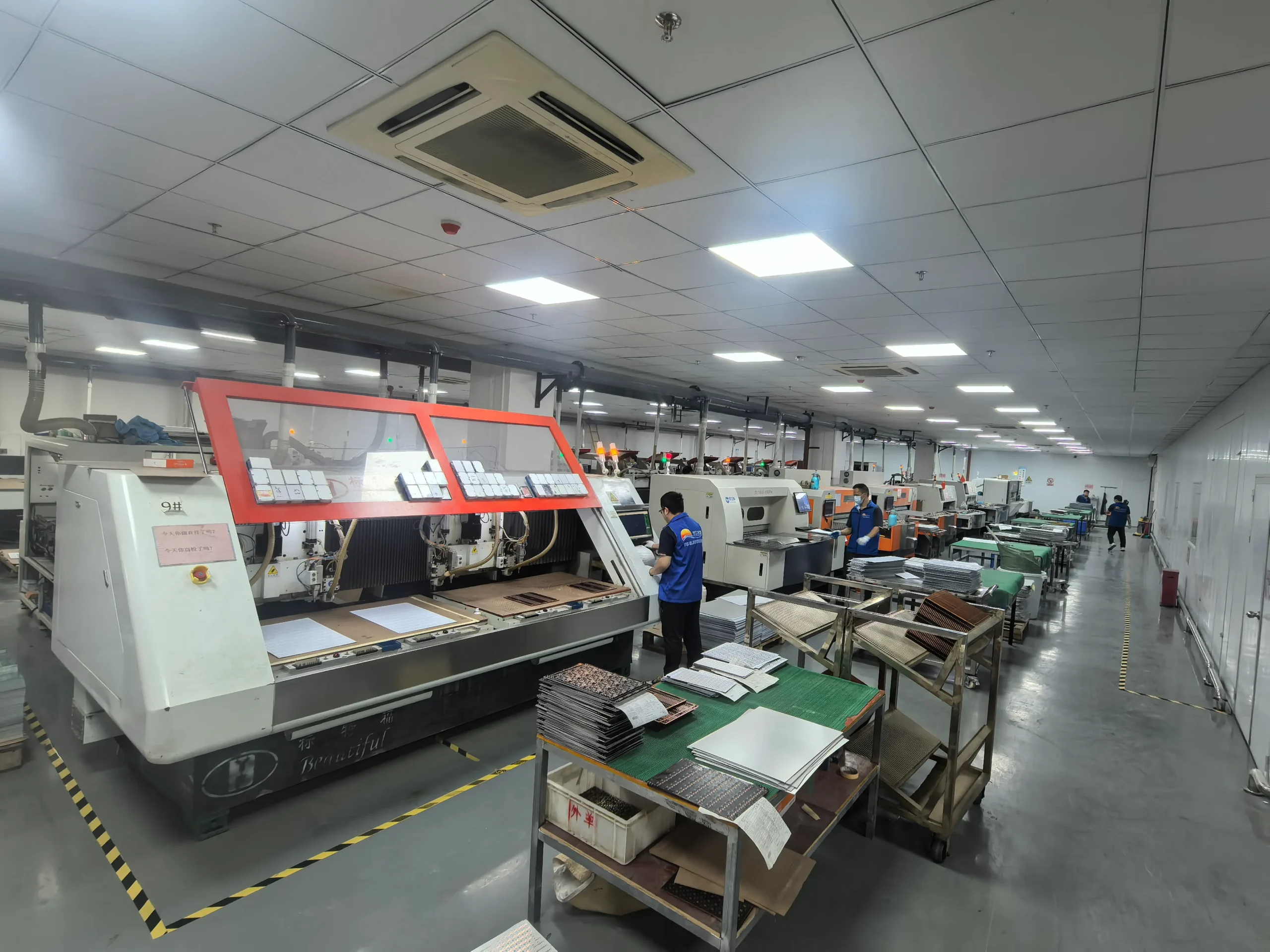
Drilling & PTH
Mechanical drilling and plated through-hole preparation.
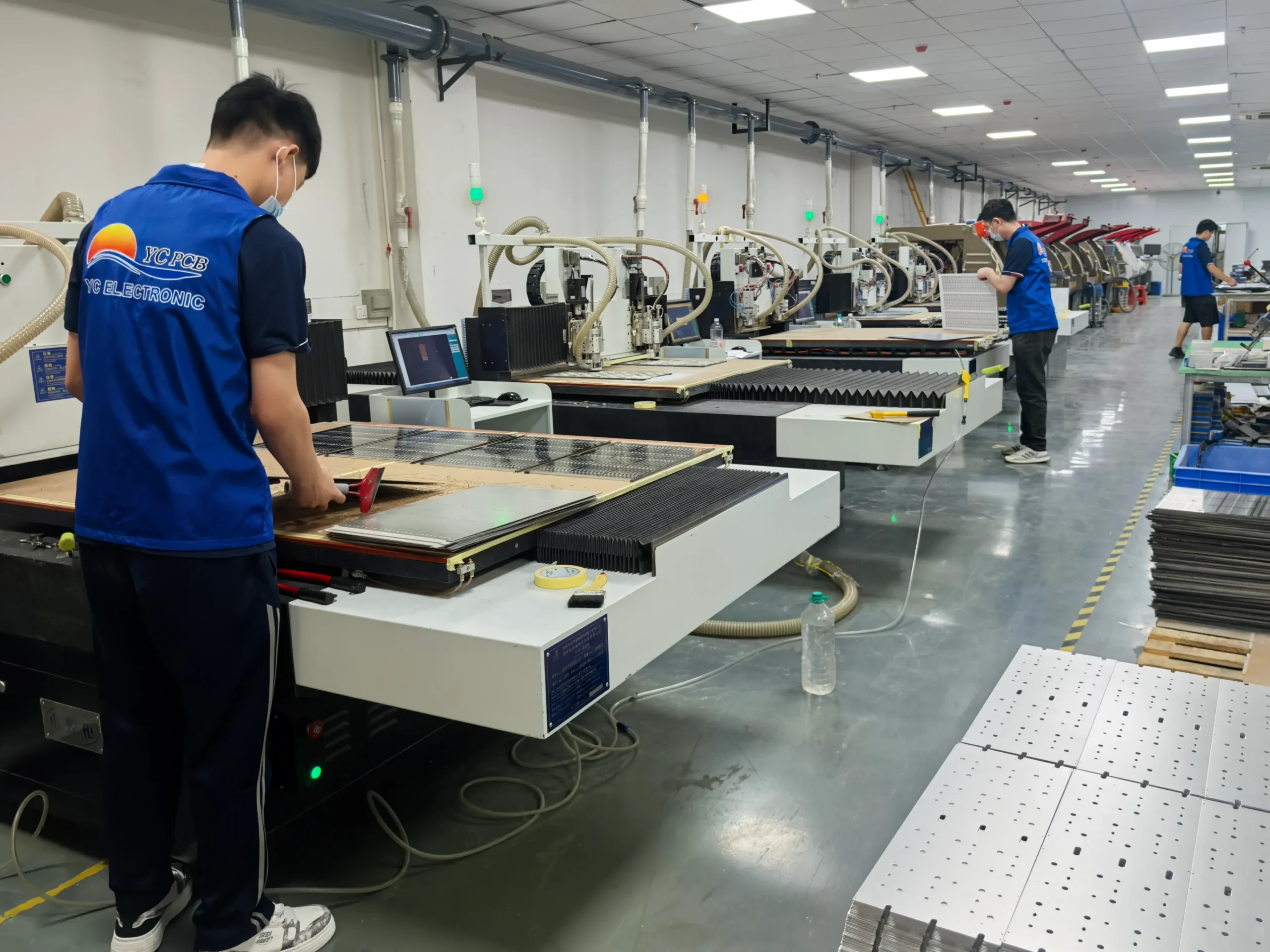
Routing & V-Cut
CNC milling, V-Cut, tab routing, and custom panel forming.
Pre-Production Design for Manufacturability Review
DFM review is part of the standard quotation and production preparation process. Before fabrication, our engineering team reviews Gerber files, drill files, via structures, annular rings, copper spacing, solder mask clearance, panelization method, surface finish, and assembly-related risks.
If design modification, stack-up adjustment, golden finger requirement, or assembly engineering support is needed, we will confirm details before proceeding.
DFM Feedback
Typical response time after receiving complete Gerber and drill files.
Via and Drill Review
Drill size, annular ring, via clearance, slot holes, and plated through-hole reliability can be reviewed.
V-Cut / Routing Review
Board outline, V-Cut, tab routing, tooling holes, and breakaway design can be checked before production.
Assembly Check
BOM, polarity, package, SMT/DIP process, test method, and packing requirement can be reviewed when assembly is required.
What Buyers Receive After DFM Review
A DFM review helps identify manufacturability risks before production release. The review can include hole size risk, annular ring issues, solder mask bridge concerns, copper clearance, panelization suggestions, and surface finish recommendations.

Sample DFM Review Items
- • Gerber and drill file completeness
- • Minimum trace / spacing review
- • Annular ring and PTH via risk
- • Solder mask bridge and opening check
- • Panelization and routing suggestion
- • Cost-impact note when process changes are required
Visual Proof of PCB Quality Control
Automated Optical Inspection
Verifies circuit pattern integrity, solder mask alignment, open/short risk, and defect classification according to IPC-A-600 Class 2 acceptance references.
Electrical Test
Net continuity and isolation are verified before packing. Test coverage depends on Gerber netlist, tooling method, and order quantity.
Visual Inspection
Reviews solder mask, surface finish, outline, board cleanliness, and final appearance.
Final Packing
Finished boards are packed according to shipping requirements, quantity, and customer packaging notes.
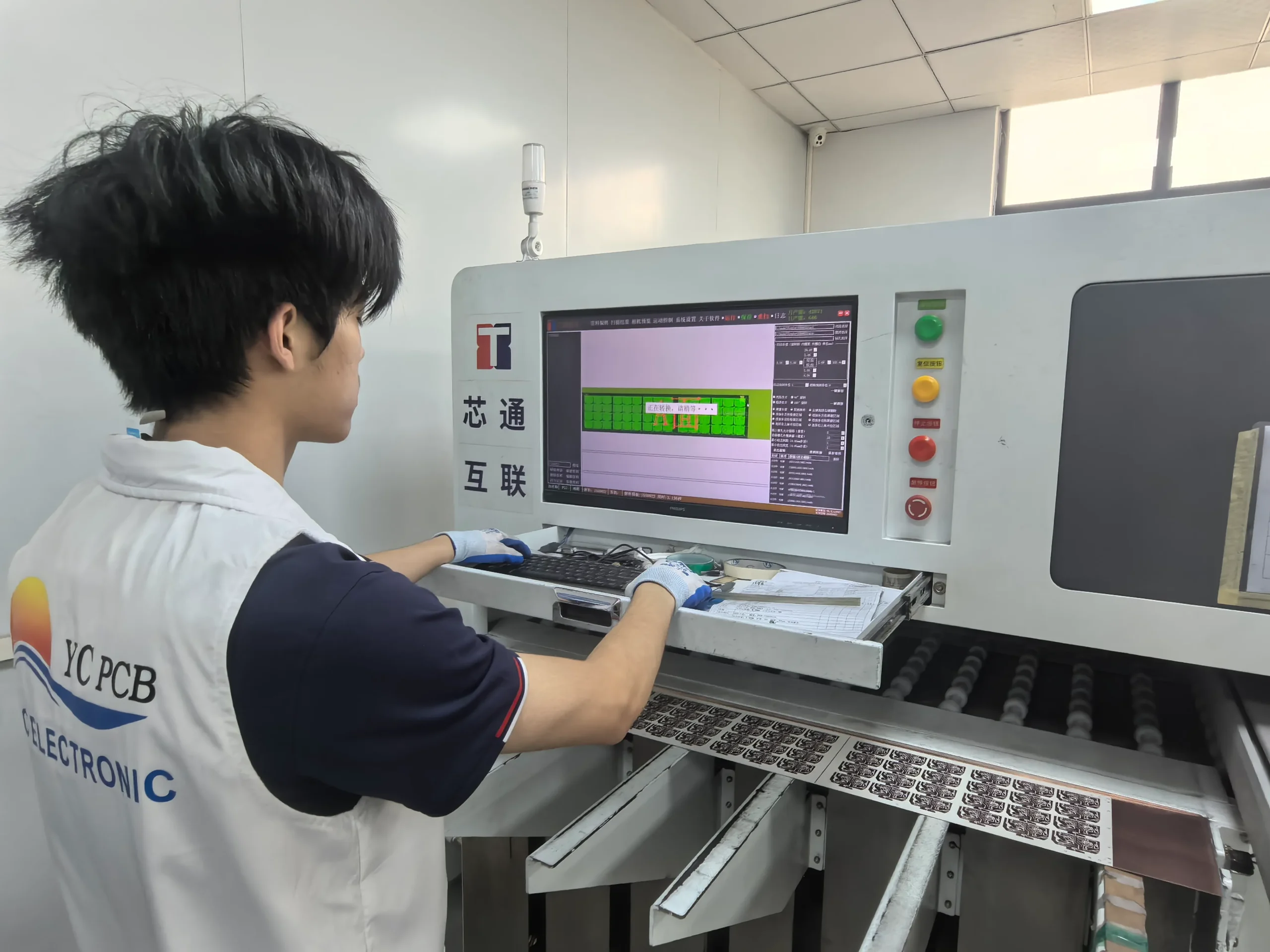
AOI Inspection
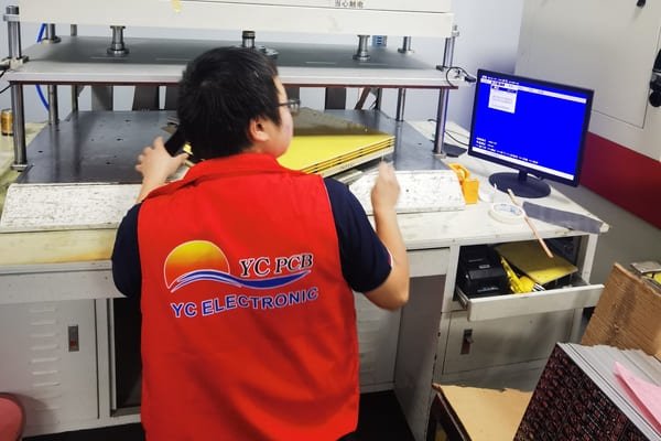
Electrical Test
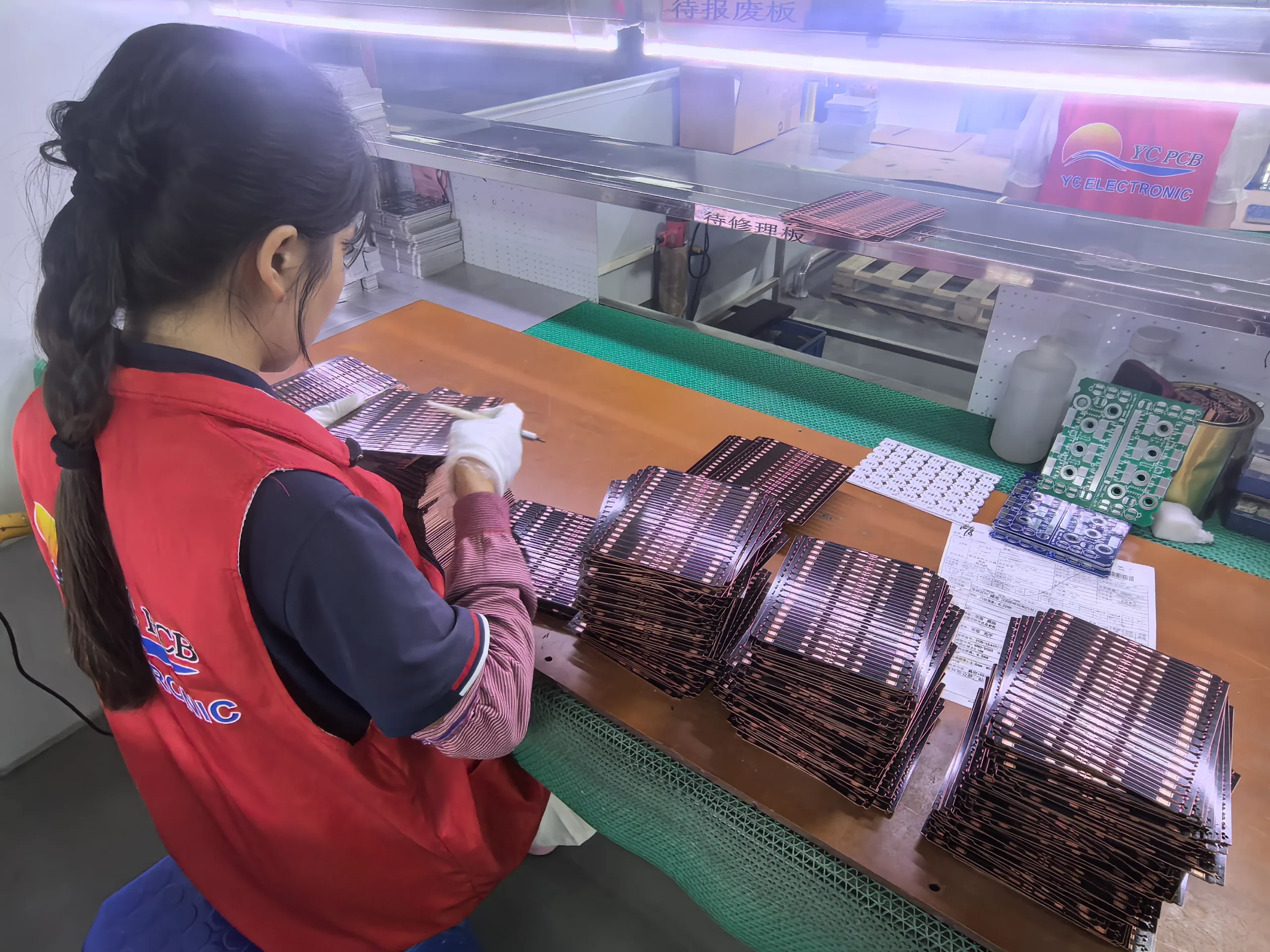
Microscope Check

Final Packing
Certification and Compliance Documentation
ISO 9001 Quality Management
Quality management documentation for production workflow, process control, inspection records, and corrective action handling.
UL Documentation Support
UL-related documentation can be provided according to project, material, laminate, and customer compliance requirements.
RoHS Compliance
RoHS compliance files and material-related documents can be prepared when required for export or customer approval.
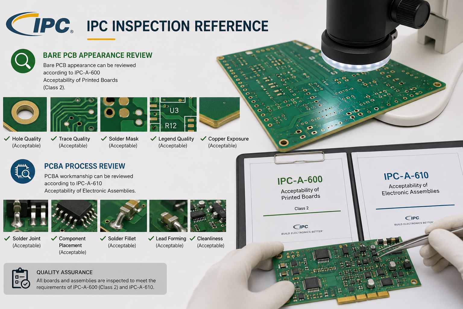
IPC Inspection Reference
Bare PCB appearance can be reviewed according to IPC-A-600 Class 2 acceptance references. PCBA workmanship can be reviewed under IPC-A-610 requirements when applicable.
Typical Use Cases for Double Sided FR4 PCB
Double sided FR4 PCB is selected when the design needs routing on both sides, plated through-hole interconnection, higher component density, or more stable signal and power routing than a single sided PCB.
Industrial Control Boards
Typical configuration: 2-layer FR4, 1-3oz copper, PTH vias, terminal holes, green solder mask, HASL or ENIG finish.
Golden Finger Connector Boards
Typical review points: finger pitch, bevel angle, gold finish, finished board thickness, insertion direction, and connector tolerance.
LED Driver / Control PCBs
Typical configuration: high-reflectance solder mask option, PTH vias, panel delivery, OSP / HASL / ENIG finish, optional SMT assembly.
Communication Interface Boards
Typical review points: signal path, routing density, ground return, connector location, surface finish, and whether 4-layer FR4 is required.
Application Scenes for Double Sided FR4 PCB
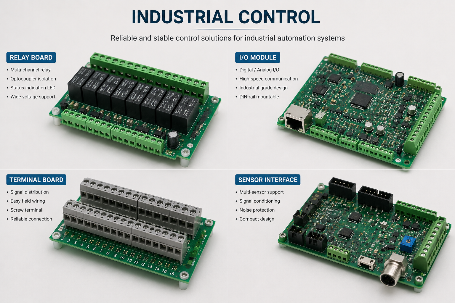
Industrial Control
Relay boards, IO modules, terminal boards, and sensor interfaces.
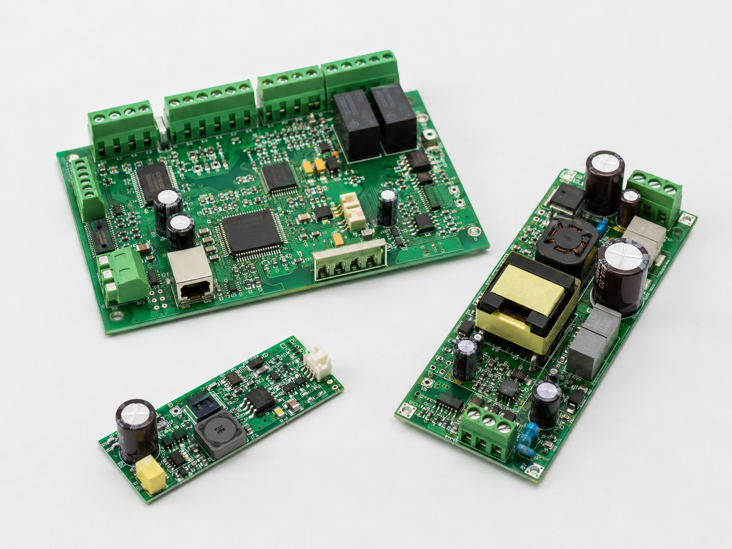
LED Driver Modules
Lighting control boards, LED driver PCBs, and LED electronic modules.
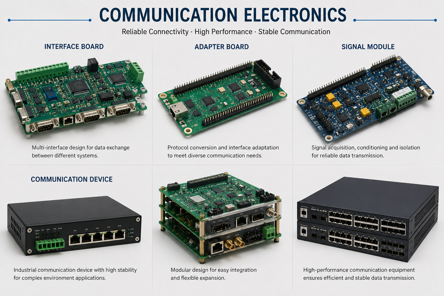
Communication Electronics
Interface boards, adapter boards, signal modules, and communication devices.
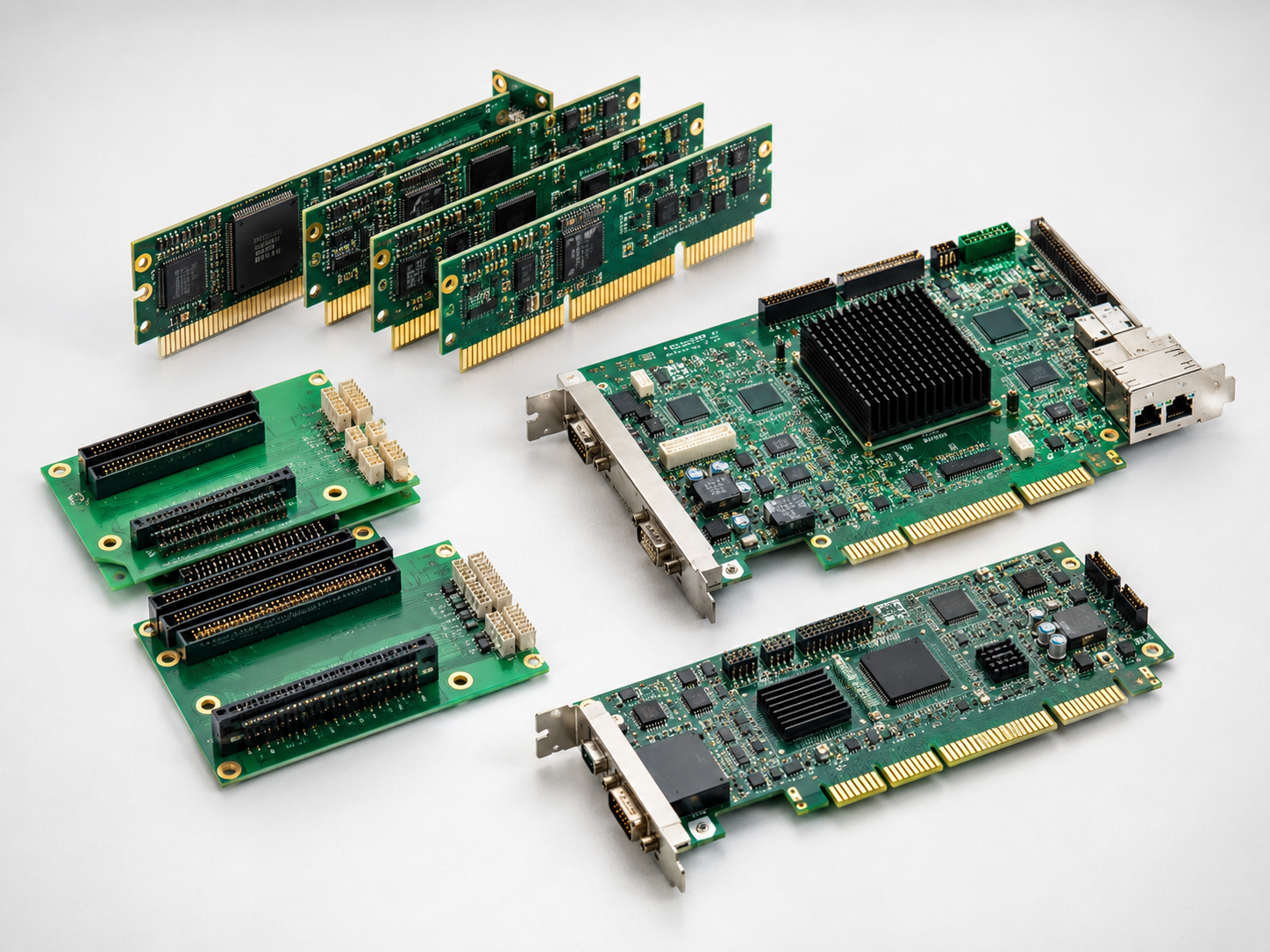
Golden Finger Modules
Plug-in modules, control cards, and connector interface boards.

Power Supply Boards
Power adapter PCBs, control power boards, and electronic power modules.

Finished PCBA
SMT, DIP, functional testing, and finished electronic control boards.
FR4, Aluminum, Copper Substrate, and LED PCBA Solutions
For LED lighting and industrial electronics, YC Electronic can also support aluminum PCB, copper substrate PCB, 4-layer FR4 PCB, and LED light PCBA projects.
FR4 PCB Series
Single layer FR4, double layer FR4, golden finger FR4, and communication series 4-layer FR4 PCB.
Aluminum PCB Series
1060 / 5052 aluminum substrate boards with 1W-8W thermal conductivity options for LED lighting and high-power modules.
Copper Substrate PCB
Purple copper substrate boards with high thermal conductivity for flashlight, projector, stage light, and high-power LED applications.
LED Light PCBA
Aluminum / FR4 PCB with component sourcing, SMT, DIP, functional testing, and packing for LED lighting products.
Gerber-Based Pricing for Double Sided FR4 PCB
Double sided FR4 PCB pricing is calculated from the Gerber file, drill file, board size, surface finish, copper weight, panel utilization, production quantity, and assembly requirement.
The following factors usually have the strongest impact on the final quotation.
The strongest pricing driver. Better panel utilization reduces material waste and unit cost.
Higher drill count increases drilling time, plating load, and inspection complexity.
HASL is the baseline cost option. ENIG is selected when pad flatness, storage stability, or golden finger requirements are important.
1oz is the common baseline. 2oz and 3oz copper increase material cost and etching control requirements.
Prototype, pilot run, and batch production are quoted separately. Volume pricing improves after panel and process conditions are stable.
Procurement, Logistics, and Delivery Support
For international PCB buyers, quotation is not only about unit price. Delivery documents, payment terms, inspection records, logistics options, and after-sales handling are also part of the purchasing decision.
Payment Terms
Standard terms are T/T before production release. For repeat customers or larger production programs, payment schedule can be reviewed based on order history, credit status, and project value.
International Logistics
DHL, UPS, FedEx, air freight, and sea freight can be reviewed according to order quantity, delivery country, packing volume, and buyer requirements.
Shipping Documents
Commercial invoice, packing list, and shipping information can be provided. RoHS or compliance documents can be prepared when required.
Inspection Records
Electrical test record, visual inspection result, and production notes can be provided based on order requirement.
After-Sales Handling
Quality issues are reviewed based on files, photos, batch records, and inspection results. Replacement or corrective action can be discussed case by case.
Request a Custom 2-Layer FR4 PCB Quote
Send Gerber files, board size, quantity, copper weight, solder mask color, surface finish, via requirement, panelization method, and PCBA files if assembly is required.
Email: sales@ycelectronic.com | Website: ycpcbs.com
Send Your Double Sided FR4 PCB Requirements
Tell us what you need. For Gerber files, drill data, BOM, pick-and-place files, drawings, golden finger details or other attachments, email them directly to sales@ycelectronic.com after submitting this form.
 English
  Japanese
  French
  German
  Spanish
  Italian
  Portuguese
  Russian
  Dutch
Dutch  Turkish