What is PCB? An Introduction to Printed Circuit Boards
A Printed Circuit Board (PCB) is the backbone of most electronic devices. But what exactly is a PCB and why is it so essential in modern technology? Understanding PCBs is key to grasping how electronic devices function. Let’s dive into the world of PCBs and explore their significance in the electronics industry.
A PCB is a flat board made from an insulating material with conductive pathways etched onto it, allowing electrical components to be connected and function together. PCBs are used in nearly every electronic device, from smartphones to medical equipment.
PCBs play a crucial role in connecting and supporting the electronic components of a device. They provide a physical platform for components and an electrical path for signals to flow, enabling the device to function.
[Table of contents]
What are the different types of PCBs?
PCBs come in a variety of designs, each tailored to meet specific needs of different applications. From simple single-layer boards to more complex multi-layer designs, there are many types of PCBs. But what are the differences between these types, and how do you choose the right one?
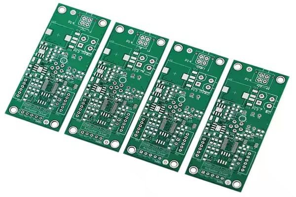
The main types of PCBs include single-sided, double-sided, and multi-layer boards. Single-sided PCBs are the simplest, while multi-layer boards allow for more complex circuits and higher performance in compact spaces.

Single-Sided PCBs
These are the most basic type of PCB, with components mounted on only one side of the board. They are typically used in low-cost and low-complexity applications.
Double-Sided PCBs
These PCBs have components mounted on both sides, allowing for more compact designs and additional functionality.
Multi-Layer PCBs
Multi-layer PCBs stack several layers of PCB material, allowing for complex circuits in a compact space. These are commonly used in high-performance electronics, such as computers and communication devices.
| PCB Type | Features |
|---|---|
| Single-Sided | Simple, low cost, used in basic electronics. |
| Double-Sided | More components, compact, medium complexity. |
| Multi-Layer | High performance, compact, complex designs. |
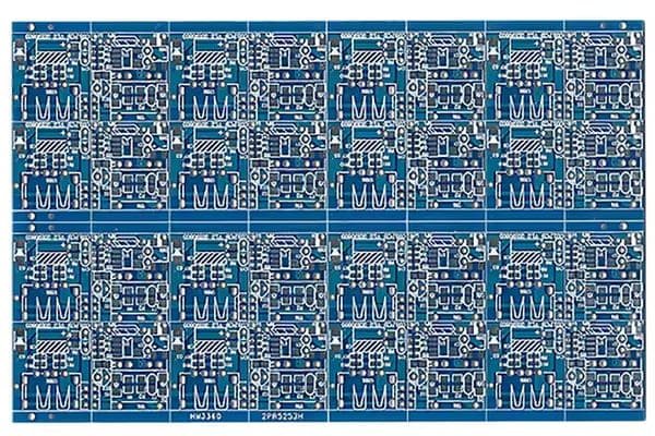
How are PCBs manufactured?
The manufacturing process of a PCB involves several key steps to ensure quality and precision. But how exactly are PCBs made, and what steps are involved in bringing them to life?
PCBs are manufactured through a process that includes designing the circuit, etching the copper tracks, drilling holes, and adding components. This is done with high precision to ensure the board functions as intended.

PCB Design
The process begins with creating a design that specifies the layout of the components and their electrical connections.
Etching
Once the design is ready, the copper layer is etched away to form the electrical pathways, leaving behind the necessary conductive tracks.
Drilling and Plating
Holes are drilled into the board to allow for the insertion of components, and plating ensures that electrical connections are made between different layers of the board.
| Manufacturing Step | Details |
|---|---|
| Design | Layout of components and connections. |
| Etching | Removal of excess copper to form circuits. |
| Drilling and Plating | Insertion of components and creation of vias. |
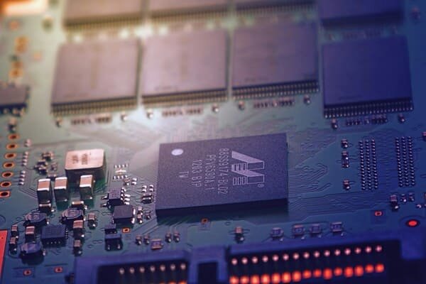
Key components of a PCB
A PCB is made up of various components that each play a crucial role in its functionality. Understanding these components is essential for anyone working with or designing PCBs. So, what are the key components that make up a PCB?
The key components of a PCB include traces, pads, vias, and components such as resistors, capacitors, and integrated circuits. Each component has a specific function that contributes to the overall performance of the PCB.

Traces and Pads
Traces are the conductive pathways that connect components, while pads are the areas where components are soldered to the PCB.
Vias
Vias are small holes that allow electrical signals to pass between layers in multi-layer PCBs.
Electronic Components
These include resistors, capacitors, and integrated circuits, which perform the electrical functions necessary for the PCB to work.
| Key Components | Function |
|---|---|
| Traces | Electrical paths between components. |
| Pads | Points where components are soldered. |
| Vias | Allow signals to pass between PCB layers. |
| Electronic Components | Perform electrical functions like resistance or amplification. |
Conclusion
In conclusion, PCBs are integral to modern electronic devices, providing a platform for electrical connections and ensuring that components work together seamlessly. Understanding the different types, manufacturing processes, and key components of PCBs can help you make informed decisions when designing or working with these critical components.