The PCB Manufacturing Process: A Step-by-Step Guide

The process of manufacturing a PCB may seem complicated, but it is crucial to ensure high-quality and reliable electronic devices. How exactly are PCBs made from design to production, and what steps are involved in ensuring their quality? Let’s break down the step-by-step process of PCB manufacturing.
The PCB manufacturing process involves several key steps, including design, material preparation, etching, and assembly. Each step is carefully controlled to ensure the final product meets the required specifications.
From design to production, each stage of the PCB manufacturing process is important to ensure the board functions properly. Let’s explore how PCBs are made and how quality control ensures their reliability.
[Table of contents]
- From design to production: How PCBs are made
- The role of CAD software in PCB design
- Quality control in PCB manufacturing
From design to production: How PCBs are made
The journey of a PCB starts with design and ends with a fully assembled board ready for use in electronic devices. But what are the key steps involved in taking a PCB from concept to reality?
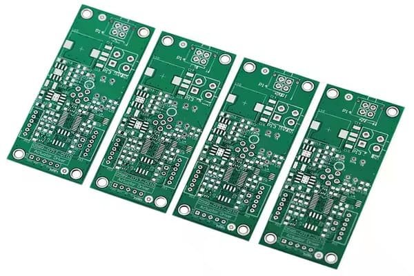
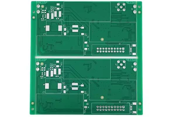
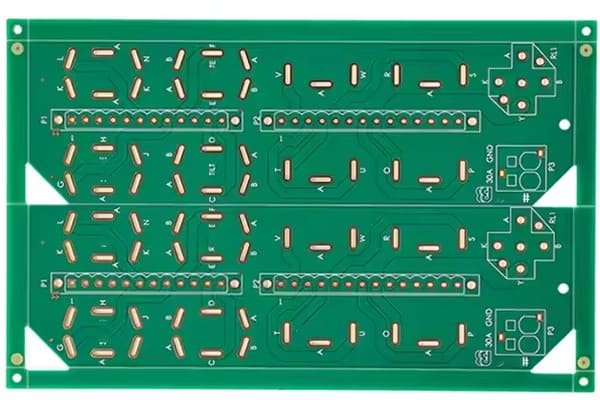
The PCB manufacturing process involves several key stages: designing the board, preparing materials, etching the copper layers, drilling holes, and assembling components. Each step ensures that the board meets its functional requirements.
Step 1: PCB Design
The first step in PCB manufacturing is designing the layout, which specifies the placement of components and connections. This is done using advanced software to create a detailed schematic.
Step 2: Material Preparation
Once the design is complete, materials like copper-clad laminate are prepared to form the base of the PCB.
Step 3: Etching
Etching removes excess copper from the material, leaving behind the conductive traces that form the electrical paths between components.
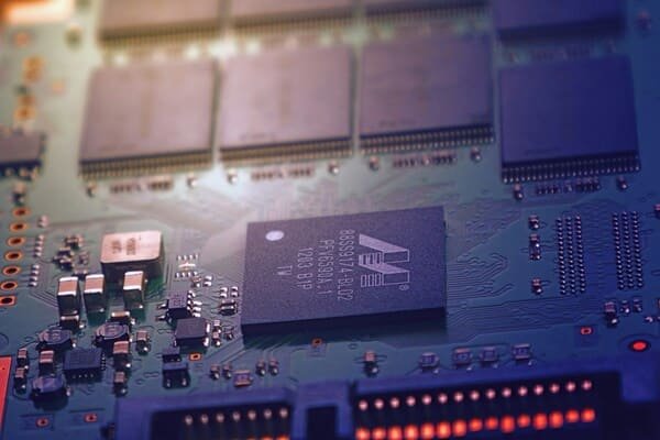
Step 4: Drilling and Plating
Holes are drilled to insert components, and plating is applied to connect different layers of the PCB.
| Manufacturing Step | Description |
|---|---|
| PCB Design | Creation of the layout and schematic. |
| Material Preparation | Preparation of copper-clad laminate. |
| Etching | Removal of excess copper to form electrical paths. |
| Drilling and Plating | Creation of holes and connections between layers. |
The role of CAD software in PCB design
Modern PCB design relies heavily on Computer-Aided Design (CAD) software. But how does CAD software fit into the design process, and what role does it play in ensuring accuracy and functionality?
CAD software is used to create a detailed digital model of the PCB. This software allows designers to plan the board layout, route electrical connections, and identify potential issues before the physical manufacturing process begins.
Planning and Layout
CAD software allows designers to carefully plan the placement of components and traces, optimizing the board for size, performance, and manufacturability.
Simulation and Testing
Before production, the design can be simulated within the CAD software to identify potential issues, such as signal interference or component placement errors.
| Role of CAD Software | Description |
|---|---|
| Planning and Layout | Design the board with optimized component placement and routing. |
| Simulation and Testing | Test the design virtually to ensure it meets specifications. |
Quality control in PCB manufacturing
Ensuring the quality of a PCB is essential to its performance and reliability. But what quality control measures are put in place to make sure that each PCB meets its required standards?
Quality control in PCB manufacturing includes inspections, testing, and compliance with industry standards. These measures are implemented throughout the manufacturing process to identify defects and ensure that each board is functional and durable.
Inspection Techniques
Inspection methods like visual inspection, Automated Optical Inspection (AOI), and X-ray inspection are used to detect defects in the PCB design, traces, and components.
Electrical Testing
PCBs are tested to ensure that they meet performance specifications, including continuity testing and functional testing to verify the integrity of electrical paths.
| Quality Control Method | Description |
|---|---|
| Visual Inspection | Detects surface defects or errors in components. |
| AOI (Automated Optical Inspection) | Checks for defects in component placement and soldering. |
| Electrical Testing | Verifies the functionality and integrity of the electrical pathways. |
Conclusion
In conclusion, the PCB manufacturing process is a multi-step procedure that involves careful design, material preparation, etching, drilling, and quality control. CAD software plays a crucial role in ensuring accurate design and functionality, while quality control measures ensure that the final product is reliable and meets the required standards. Each of these steps is vital to producing a high-quality PCB that will perform effectively in electronic devices.