 Skip to content
Introduction:
Printed Circuit Board (PCB) assembly is a critical process in the manufacturing of electronic devices, enabling the interconnection of various electronic components to create functional and reliable devices. Whether it's a smartphone, a computer, or an advanced industrial machine, PCB assembly plays a vital role in bringing these devices to life. This article provides a comprehensive guide to PCB assembly, covering the key stages involved in transforming a design into a fully functional PCB assembly.
Design Phase:
The journey of a PCB assembly begins with the design phase. During this stage, electrical engineers and designers create the schematic diagram and layout of the PCB using specialized software tools. They define the component placement, routing paths, and signal traces to ensure proper functionality and signal integrity.
Component Selection and Procurement:
Once the design is finalized, the next step is selecting the electronic components that will be mounted on the PCB. Component selection involves considering factors such as functionality, reliability, availability, and cost. After the components are chosen, they need to be procured from reliable suppliers or distributors.
PCB Fabrication:
With the components in hand, the PCB fabrication process begins. This involves producing the actual circuit board based on the design specifications. The fabrication process typically includes steps such as substrate material selection, layer stacking, etching, drilling, plating, and soldermask application. Advanced fabrication techniques, such as multilayer PCBs and surface-mount technology (SMT), are commonly used to accommodate complex designs and miniaturized components.
Component Placement:
Once the PCBs are fabricated, the next stage is component placement. This step involves precisely positioning the electronic components onto the PCB using automated equipment or manual labor, depending on the scale of production. Surface-mount technology (SMT) is widely used due to its high efficiency, accuracy, and ability to handle miniaturized components. Through-hole technology (THT) is an alternative method used for larger components or specific applications.
Soldering and Reflow:
After component placement, soldering is performed to establish electrical and mechanical connections between the components and the PCB. Solder paste, a mixture of solder alloy particles and flux, is applied to the solder pads. The PCB is then subjected to a reflow process, where it is heated to melt the solder paste, creating strong and reliable solder joints. Various methods, such as infrared heating, vapor phase, or convection reflow, are used depending on the production requirements.
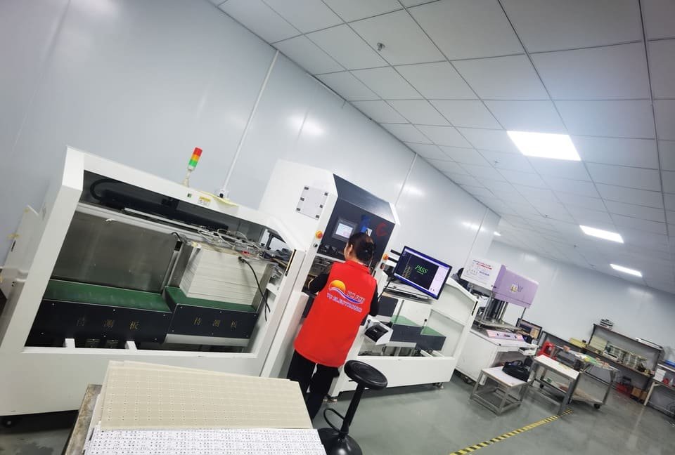
Inspection and Testing:
Quality control is a crucial aspect of PCB assembly. Once the soldering process is complete, the assembled PCBs undergo thorough inspection and testing. Automated optical inspection (AOI) systems are commonly used to detect defects such as misalignment, missing components, solder bridges, or open circuits. Functional testing is also conducted to ensure that the PCB operates as intended, verifying the electrical connections, signal integrity, and overall performance.
Packaging and Delivery:
After inspection and testing, the PCB assemblies are prepared for packaging and delivery. This involves cleaning the PCBs, removing any flux residues, and applying conformal coatings or protective films to enhance durability and reliability. The finished PCB assemblies are then carefully packaged, ready to be integrated into the final electronic devices or delivered to customers.
Conclusion:
PCB assembly is a complex and critical process that brings electronic devices to life. From the initial design phase to the final packaging and delivery, each stage requires precision, attention to detail, and adherence to quality standards. By following the comprehensive guide outlined in this article, manufacturers can ensure the successful assembly of PCBs, resulting in functional, reliable, and high-quality electronic devices that power our modern world.
