
How can you improve the efficiency and quality of PCB design?

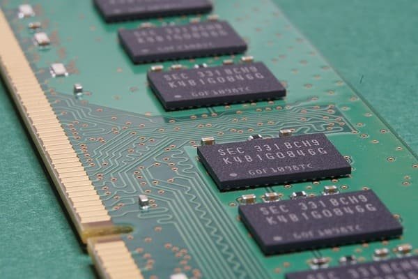
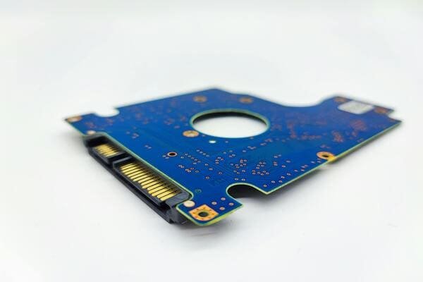
Designing printed circuit boards (PCBs) is a complex task that requires precision and efficiency. Many engineers and manufacturers struggle with optimizing their PCB designs to meet performance standards while minimizing production time and costs. These challenges can lead to delays, increased expenses, and subpar product quality. However, by focusing on key aspects of the design process and leveraging modern tools, it's possible to enhance both the efficiency and quality of PCB designs.
Improving the efficiency and quality of PCB design involves considering important design factors, utilizing advanced design software for accuracy, and implementing thorough testing and verification processes.
Enhancing PCB design not only streamlines production but also ensures reliable and high-performing electronic products.
[Table of contents]
- What are the important considerations in PCB design?
- How can modern design software improve design accuracy?
- How does testing and verification ensure the design is correct?
- Conclusion
What are the important considerations in PCB design?
Designing an efficient and high-quality PCB requires careful attention to several critical factors that influence the board's performance and manufacturability.
Key considerations in PCB design include component placement, signal integrity, thermal management, and manufacturability.
Addressing these factors from the outset ensures that the PCB meets both functional and production requirements.

Component Placement
Strategically placing components on the PCB minimizes signal path lengths and reduces electromagnetic interference (EMI). Proper placement also facilitates easier routing and assembly.
Signal Integrity
Maintaining signal integrity is essential for high-speed and high-frequency PCB designs. This involves careful routing of traces, impedance matching, and minimizing crosstalk between signals.
| Consideration | Importance | Best Practices |
|---|---|---|
| Component Placement | Reduces signal path lengths and EMI | Group related components, minimize distance between connected parts |
| Signal Integrity | Ensures reliable data transmission | Use controlled impedance, differential pairs, and proper grounding |
| Thermal Management | Prevents overheating and ensures longevity | Incorporate thermal vias, heatsinks, and adequate spacing |
| Manufacturability | Facilitates easy production and assembly | Design for standard manufacturing processes, avoid complex geometries |
Thermal Management
Effective thermal management prevents excessive heat buildup, which can degrade component performance and shorten PCB lifespan. Techniques include using thermal vias, heatsinks, and appropriate material selection.
Manufacturability
Designing with manufacturability in mind ensures that the PCB can be produced efficiently and cost-effectively. This involves adhering to standard design rules, avoiding overly complex layouts, and selecting suitable materials.
How can modern design software improve design accuracy?
Modern PCB design software offers advanced tools and features that significantly enhance the accuracy and efficiency of the design process.
Utilizing modern design software improves design accuracy by providing precise layout tools, automated error checking, and simulation capabilities that help identify and rectify potential issues early in the design phase.
These software solutions streamline the design process, reduce human error, and ensure that PCBs meet stringent quality standards.
Precise Layout Tools
Advanced layout tools allow for exact placement of components and routing of traces, ensuring that design specifications are met with high precision.
Automated Error Checking
Automated error checking features help identify design rule violations, electrical inconsistencies, and potential manufacturing issues, enabling designers to address problems before production begins.
| Feature | Benefit | Example Tools |
|---|---|---|
| Precise Layout Tools | Ensures accurate component placement and routing | Altium Designer, KiCad, Eagle |
| Automated Error Checking | Reduces design errors and improves reliability | Design rule checks (DRC), electrical rule checks (ERC) |
| Simulation Capabilities | Allows testing of signal integrity and thermal performance | SPICE simulations, thermal analysis tools |
| Collaboration Features | Enhances teamwork and design consistency | Cloud-based platforms, version control |
Simulation Capabilities
Simulation tools enable designers to test the electrical and thermal performance of the PCB under various conditions, allowing for optimization before physical prototypes are made.
Collaboration Features
Modern design software often includes collaboration features that facilitate teamwork, ensuring that all team members are working with the most up-to-date design information.
How does testing and verification ensure the design is correct?
Thorough testing and verification are essential steps in the PCB design process that confirm the board functions as intended and meets all specified requirements.
Implementing comprehensive testing and verification processes ensures that PCB designs are free from defects, perform reliably under expected conditions, and comply with industry standards.
These processes help in delivering high-quality PCBs that meet customer expectations and reduce the likelihood of costly post-production fixes.
Prototype Testing
Creating and testing prototypes allows designers to evaluate the functionality and performance of the PCB in real-world conditions, identifying any necessary adjustments before mass production.
Design for Testing (DFT)
Incorporating DFT principles during the design phase facilitates easier testing and troubleshooting, enhancing overall design reliability and maintainability.
| Testing Method | Purpose | Tools/Techniques |
|---|---|---|
| Prototype Testing | Validates functionality and performance | Functional testing, environmental testing |
| Design for Testing (DFT) | Simplifies the testing process and improves reliability | Test points, boundary scan, built-in self-test (BIST) |
| Automated Optical Inspection (AOI) | Detects manufacturing defects and assembly issues | High-resolution cameras, image processing software |
| In-Circuit Testing (ICT) | Verifies electrical performance and component placement | Bed-of-nails testers, flying probe testers |
Automated Optical Inspection (AOI)
AOI systems use high-resolution cameras and image processing software to inspect PCBs for defects such as missing components, incorrect placements, and soldering issues, ensuring high manufacturing quality.
In-Circuit Testing (ICT)
ICT involves testing the electrical performance of the PCB by checking each component and connection, ensuring that the board operates correctly before it is deployed.
Conclusion
Improving the efficiency and quality of PCB design is fundamental to producing reliable and high-performing electronic products. By considering crucial design factors, leveraging modern design software for enhanced accuracy, and implementing rigorous testing and verification processes, designers can optimize their PCB designs for both performance and manufacturability. As a dedicated PCB manufacturer, we prioritize these best practices to deliver top-quality custom PCBs that meet the diverse needs of our global customers, supporting their success in a competitive market.